鈥?/div>
5 LVCMOS outputs for processor and other system circuitry
3 Buffered 25-MHz reference clock outputs
Crystal oscillator or external reference input
25-MHz input reference frequency
Selectable output frequencies include: 25, 33, 50, or 66 MHz
Low cycle-to-cycle and period jitter
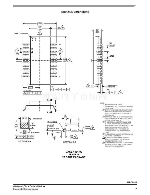
Package: 20-lead SSOP
3.3-V supply
Supports computing, networking, and telecommunications applications
Ambient temperature range: 鈥?0擄C to +85擄C
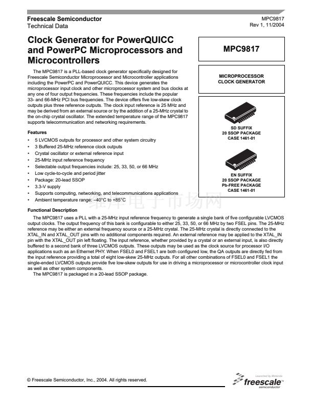
MPC9817
MICROPROCESSOR
CLOCK GENERATOR
SD SUFFIX
20 SSOP PACKAGE
CASE 1461-01
EN SUFFIX
20 SSOP PACKAGE
Pb-FREE PACKAGE
CASE 1461-01
Functional Description
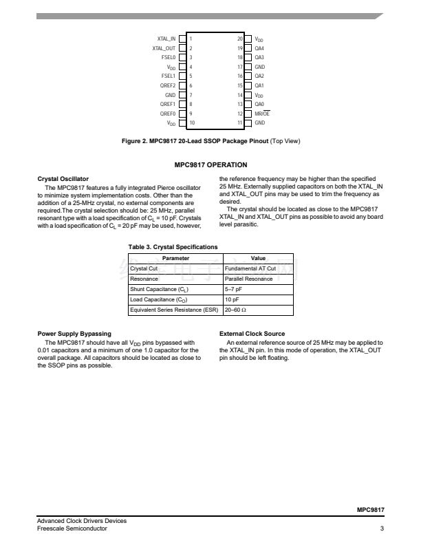
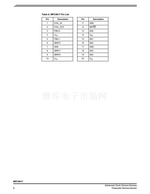
The MPC9817 uses a PLL with a 25-MHz input reference frequency to generate a single bank of five configurable LVCMOS
output clocks. The output frequency of this bank is configurable to either 25, 33, 50, or 66 MHz by two FSEL pins. The 25-MHz
reference may be either an external frequency source or a 25-MHz crystal. The 25-MHz crystal is directly connected to the
XTAL_IN and XTAL_OUT pins with no additional components required. An external reference may be applied to the XTAL_IN
pin with the XTAL_OUT pin left floating. The input reference, whether provided by a crystal or an external input, is also directly
buffered to a second bank of three LVCMOS outputs. These outputs may be used as the clock source for processor I/O
applications such as an Ethernet PHY. When FSEL0 and FSEL1 are both configured low, the QA outputs are directly fed from
the input reference providing a total of eight low-skew 25-MHz outputs. For all other combinations of FSEL0 and FSEL1 the
single-ended LVCMOS outputs provide five low-skew outputs for use in driving a microprocessor or microcontroller clock input
as well as other system components.
The MPC9817 is packaged in a 20-lead SSOP package.
漏 Freescale Semiconductor, Inc., 2004. All rights reserved.


 1
1
 2
2
 3
3
 4
4
 5
5
 6
6
 7
7
 8
8
