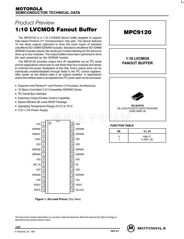
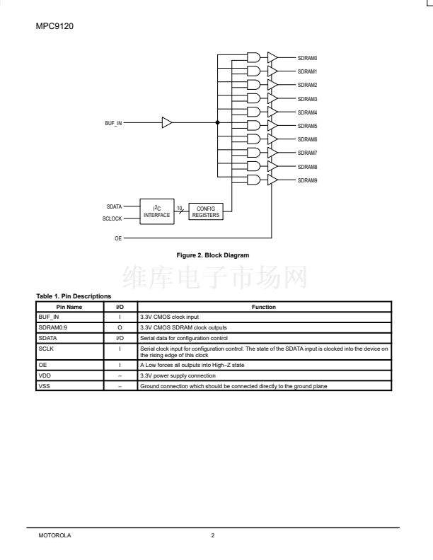
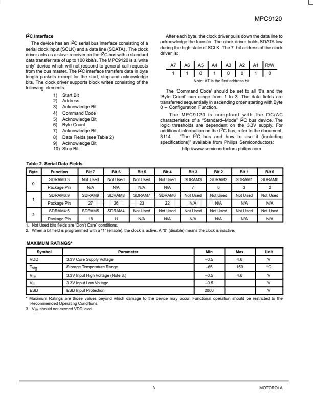
MPC9120
APPLICATIONS INFORMATION
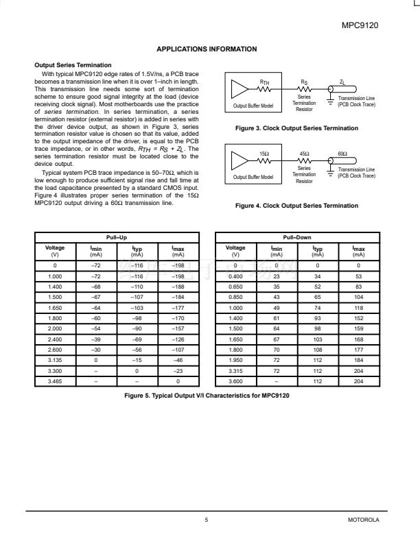
Output Series Termination
With typical MPC9120 edge rates of 1.5V/ns, a PCB trace
becomes a transmission line when it is over 1鈥搃nch in length.
This transmission line needs some sort of termination
scheme to ensure good signal integrity at the load (device
receiving clock signal). Most motherboards use the practice
of
series termination.
In series termination, a series
termination resistor (external resistor) is added in series with
the driver device output, as shown in Figure 3, series
termination resistor value is chosen so that its value, added
to the output impedance of the driver, is equal to the PCB
trace impedance, or in other words,
RTH = RS + ZL
. The
series termination resistor must be located close to the
device output.
Typical system PCB trace impedance is 50鈥?0鈩? which is
low enough to produce sufficient signal rise and fall time at
the load capacitance presented by a standard CMOS input.
Figure 4 illustrates proper series termination of the 15鈩?/div>
MPC9120 output driving a 60鈩?transmission line.
RTH
RS
Series
Termination
Resistor
ZL
Transmission Line
(PCB Clock Trace)
Output Buffer Model
Figure 3. Clock Output Series Termination
15鈩?/div>
45鈩?/div>
Series
Termination
Resistor
60鈩?/div>
Transmission Line
(PCB Clock Trace)
Output Buffer Model
Figure 4. Clock Output Series Termination
Pull鈥揢p
Voltage
(V)
0
1.000
1.400
1.500
1.650
1.800
2.000
2.400
2.600
3.135
3.300
3.465
Imin
(mA)
鈥?2
鈥?2
鈥?8
鈥?7
鈥?4
鈥?0
鈥?4
鈥?9
鈥?0
0
鈥?/div>
鈥?/div>
Ityp
(mA)
鈥?16
鈥?16
鈥?10
鈥?07
鈥?03
鈥?8
鈥?0
鈥?9
鈥?6
鈥?5
0
鈥?/div>
Imax
(mA)
鈥?98
鈥?98
鈥?88
鈥?84
鈥?77
鈥?70
鈥?57
鈥?26
鈥?07
鈥?6
鈥?3
0
Voltage
(V)
0
0.400
0.650
0.850
1.000
1.400
1.500
1.650
1.800
1.950
3.315
3.600
Imin
(mA)
0
23
35
43
49
61
64
67
70
72
72
鈥?/div>
Pull鈥揇own
Ityp
(mA)
0
34
52
65
74
93
98
103
108
112
112
112
Imax
(mA)
0
53
83
104
118
152
159
168
177
184
204
204
Figure 5. Typical Output V/I Characteristics for MPC9120
TIMING SOLUTIONS
BR1333 鈥?REV 5
5
MOTOROLA
MPC9120相關(guān)型號PDF文件下載
-
型號
版本
描述
廠商
下載
-
英文版
Motorola, Inc [1:6 PCI CLOCK GENERATOR/ FANOUT BUFFER]
-
英文版
1:6 PCI CLOCK GENERATOR/ FANOUT BUFFER
-
英文版
1:6 PCI Clock Qenerator/Fanout Buffer
-
英文版
Motorola, Inc [LOW VOLTAGE CMOS 1:18 CLOCK DISTRIBUTION CHI...
-
英文版
Motorola, Inc [LOW-VOLTAGE 1:9 DIFFERENTIAL ECL/HSTL TO HST...
-
英文版
Low Voltage PLL Clock Drlver
-
英文版
Low Voltage PLL Clock Drlver
-
英文版
Motorola, Inc [LOW VOLTAGE PLL CLOCK DRIVER]
-
英文版
Motorola, Inc [LOW VOLTAGE 1:18 CLOCK DISTRIBUTION CHIP]
-
英文版
Low Voltage 1:27 Clock Dlstrlbutlon Chlp
-
英文版
Motorola, Inc [LOW VOLTAGE 1:10 CMOS CLOCK DRIVER]
-
英文版
Motorola, Inc [LOW VOLTAGE 1:9 CLOCK DISTRIBUTION CHIP]
-
英文版
Motorola, Inc [LOW VOLTAGE 1:12 CLOCK DISTRIBUTION CHIP]
-
英文版
Motorola, Inc [LOW VOLTAGE 1:15 PECL TO CMOS CLOCK DRIVER]
-
英文版
Low Voltage PLL Clock Drlver
-
英文版
Low Voltage PLL Clock Drlver
-
英文版
Low Voltage PLL Clock Drlver
-
英文版
Low Voltage PLL Clock Drlver
-
英文版
Low Voltage PLL Clock Drlver
-
英文版
Low Voltage PLL Clock Drlver


 1
1
 2
2
 3
3
 4
4
 5
5
 6
6
