LC75394NE
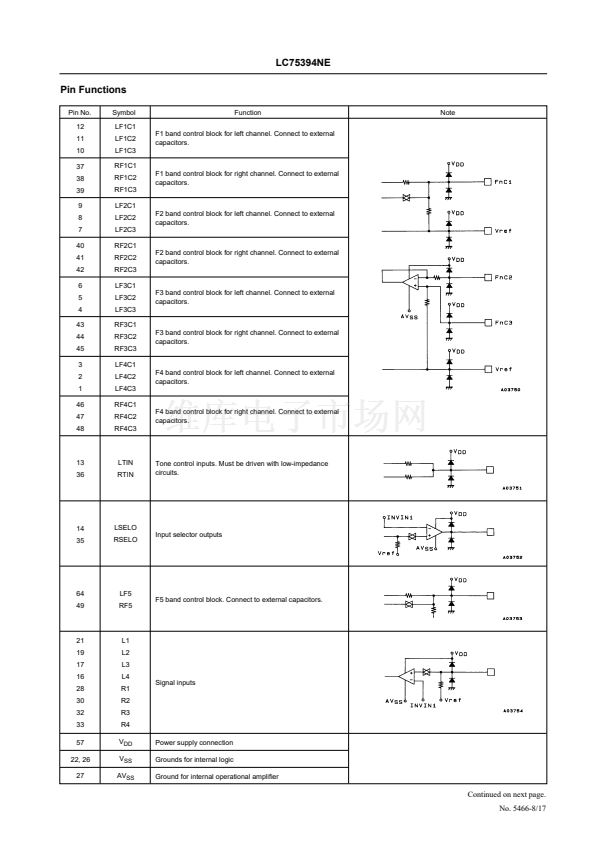
Continued from preceding page.
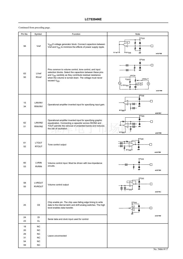
Pin No.
Symbol
Function
Note
56
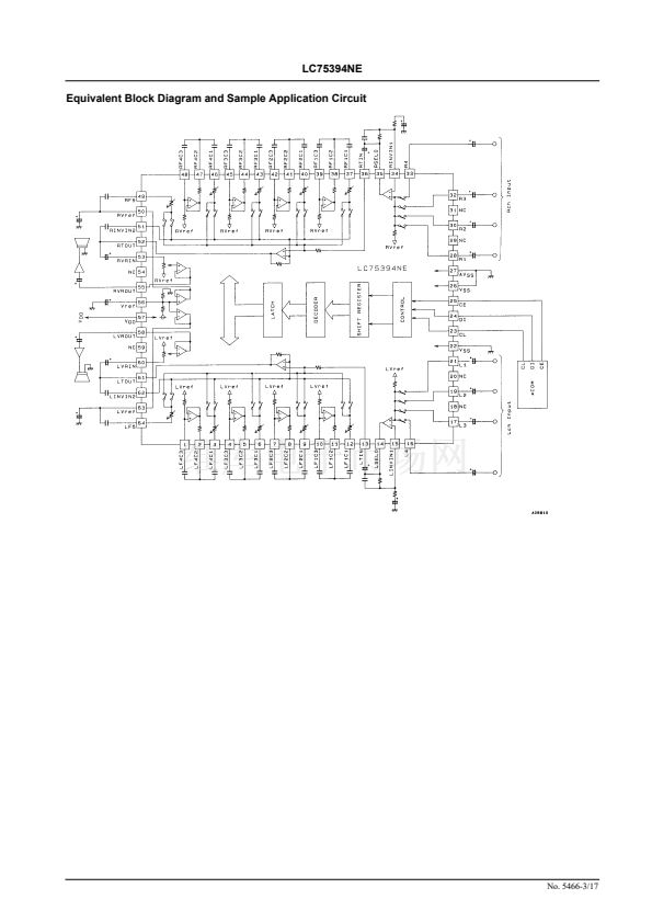
Vref
V
DD
/2 voltage generator block. Connect capacitors between
Vref and V
SS
to minimize the effects of power supply ripple.
63
50
LVref
RVref
Pins common to volume control, tone control, and input
selection blocks. Select the capacitors between these pins
and V
SS
carefully as they contribute residual resistance
when the volume is turned down. The voltage must never
exceed V
DD
.
15
34
LINVIN1
RINVIN1
Operational amplifier inverted input for specifying input gain.
62
51
LINVIN2
RINVIN2
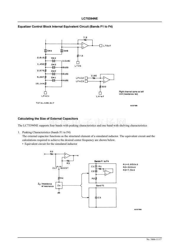
Operational amplifier inverted input for specifying graphic
equalization. Connecting a capacitor across INVIN2 and
TOUT permits the removal of unwanted bands and reduces
the risk of oscillation.
61
52
LTOUT
RTOUT
Tone control output
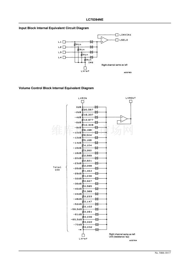
60
53
LVRIN
RVRIN
Volume control input. Must be driven with low-impedance
circuits.
58
55
LVROUT
RVROUT
Volume control output
25
CE
Chip enable pin. The chip uses falling edge timing to write
data to the internal latch and shift analog switches. The high
level enables data transfer.
24
23
18
20
29
31
54
59
DI
CL
NC
NC
NC
NC
NC
NC
Serial data and clock input used for control
Leave unconnected
No. 5466-9/17


 1
1
 2
2
 3
3
 4
4
 5
5
 6
6
 7
7
 8
8
 9
9
 10
10
 11
11
 12
12
 13
13
 14
14
 15
15
 16
16
 17
17
