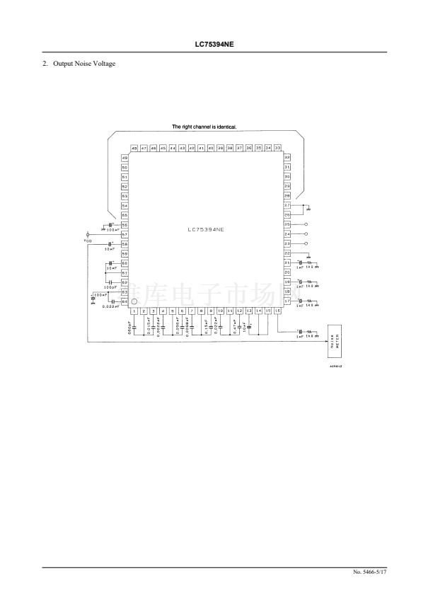
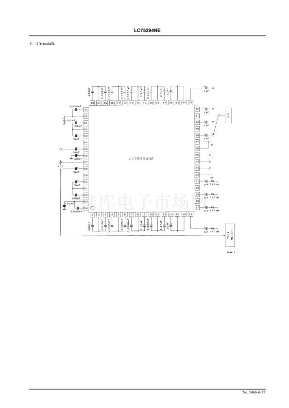
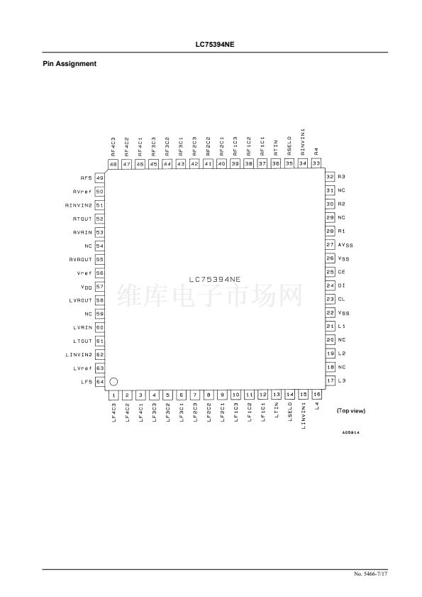
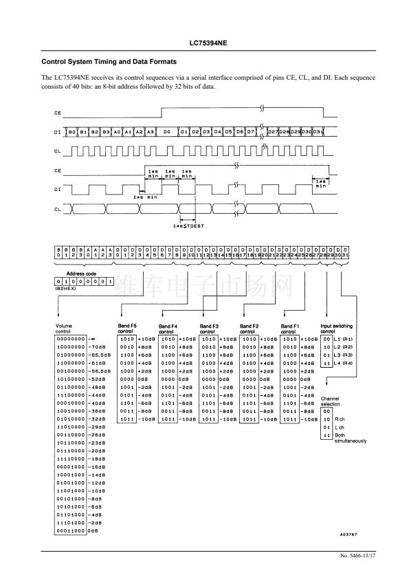
LC75394NE
Pin Functions
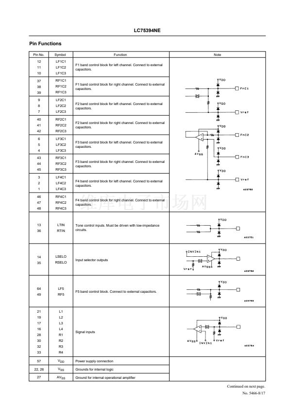
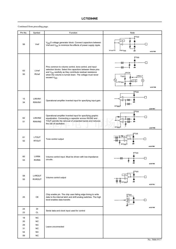
Pin No.
12
11
10
37
38
39
9
8
7
40
41
42
6
5
4
43
44
45
3
2
1
46
47
48
Symbol
LF1C1
LF1C2
LF1C3
RF1C1
RF1C2
RF1C3
LF2C1
LF2C2
LF2C3
RF2C1
RF2C2
RF2C3
LF3C1
LF3C2
LF3C3
RF3C1
RF3C2
RF3C3
LF4C1
LF4C2
LF4C3
RF4C1
RF4C2
RF4C3
F4 band control block for right channel. Connect to external
capacitors.
F4 band control block for left channel. Connect to external
capacitors.
F3 band control block for right channel. Connect to external
capacitors.
F3 band control block for left channel. Connect to external
capacitors.
F2 band control block for right channel. Connect to external
capacitors.
F2 band control block for left channel. Connect to external
capacitors.
F1 band control block for right channel. Connect to external
capacitors.
F1 band control block for left channel. Connect to external
capacitors.
Function
Note
13
36
LTIN
RTIN
Tone control inputs. Must be driven with low-impedance
circuits.
14
35
LSELO
RSELO
Input selector outputs
64
49
LF5
RF5
F5 band control block. Connect to external capacitors.
21
19
17
16
28
30
32
33
57
22, 26
27
L1
L2
L3
L4
R1
R2
R3
R4
V
DD
V
SS
AV
SS
Power supply connection
Grounds for internal logic
Ground for internal operational amplifier
Signal inputs
Continued on next page.
No. 5466-8/17


 1
1
 2
2
 3
3
 4
4
 5
5
 6
6
 7
7
 8
8
 9
9
 10
10
 11
11
 12
12
 13
13
 14
14
 15
15
 16
16
 17
17
