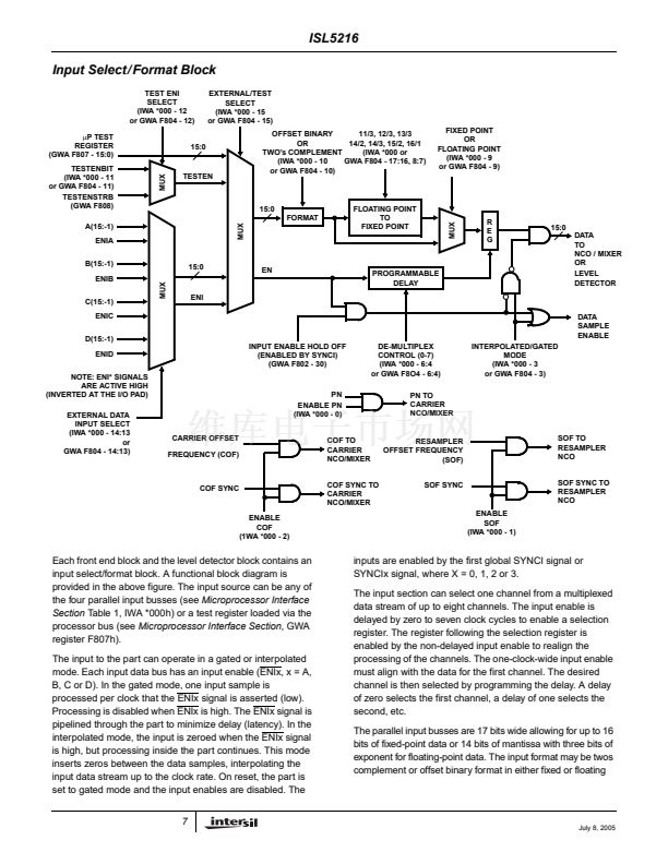
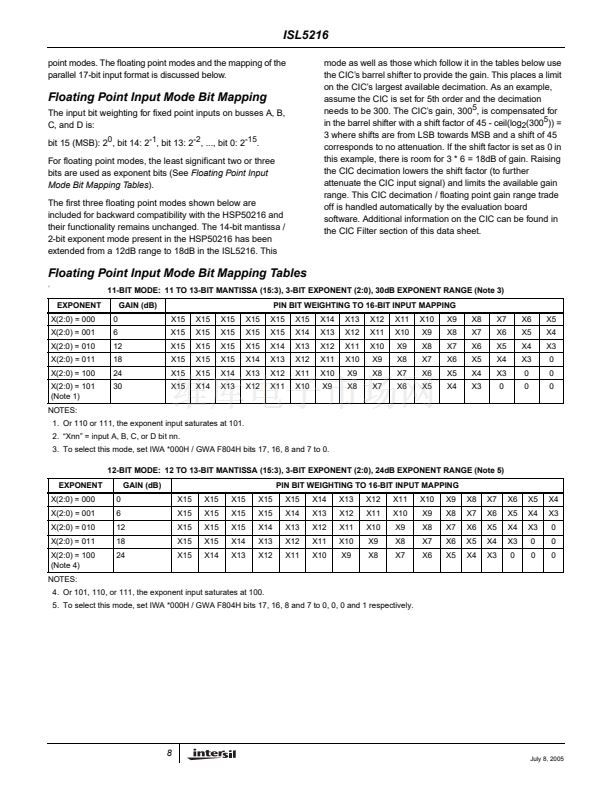
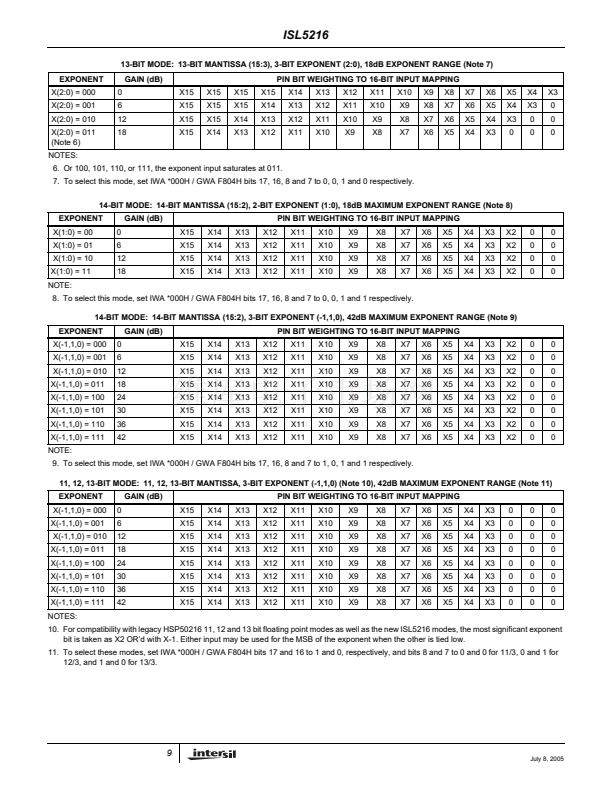
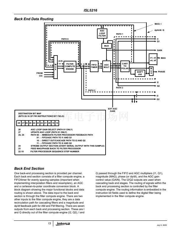
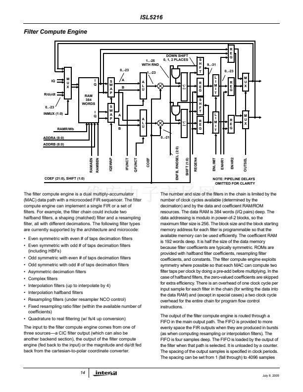
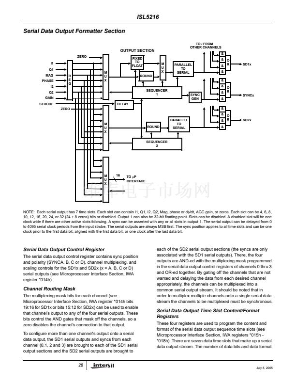
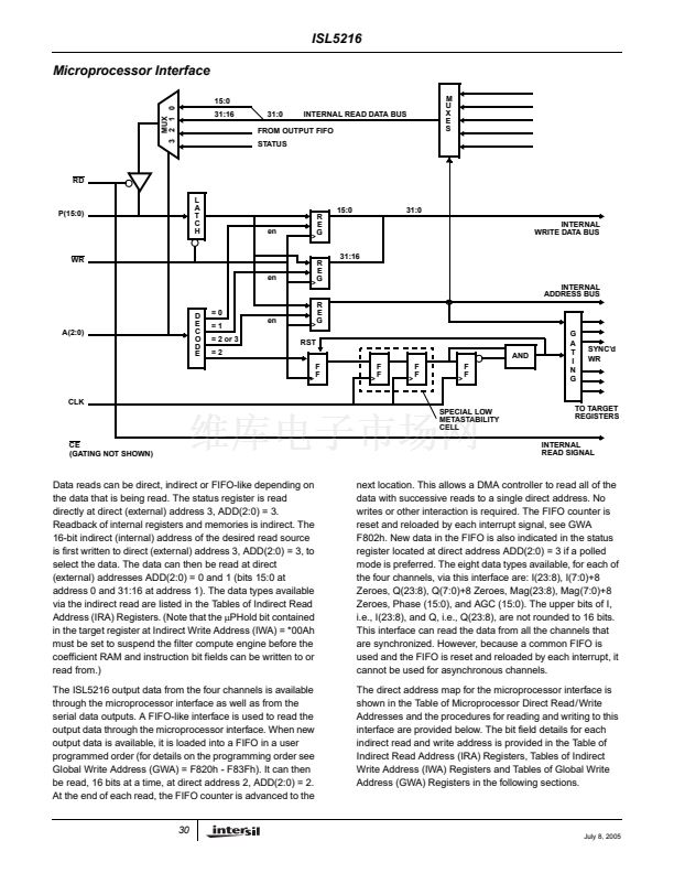
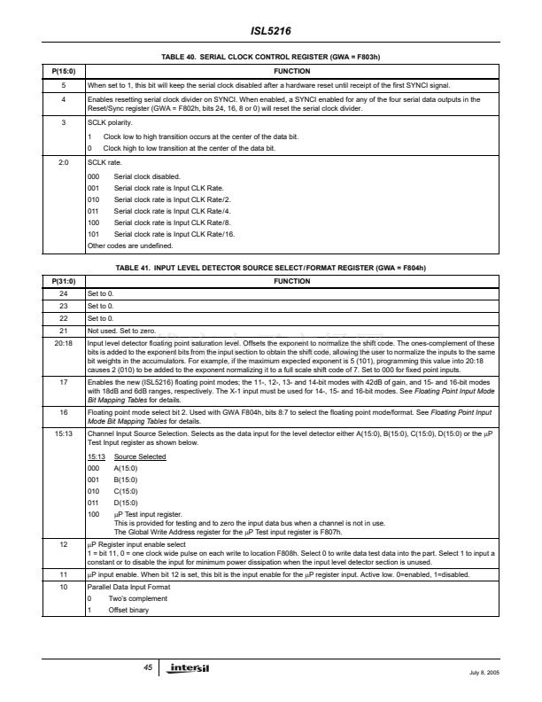
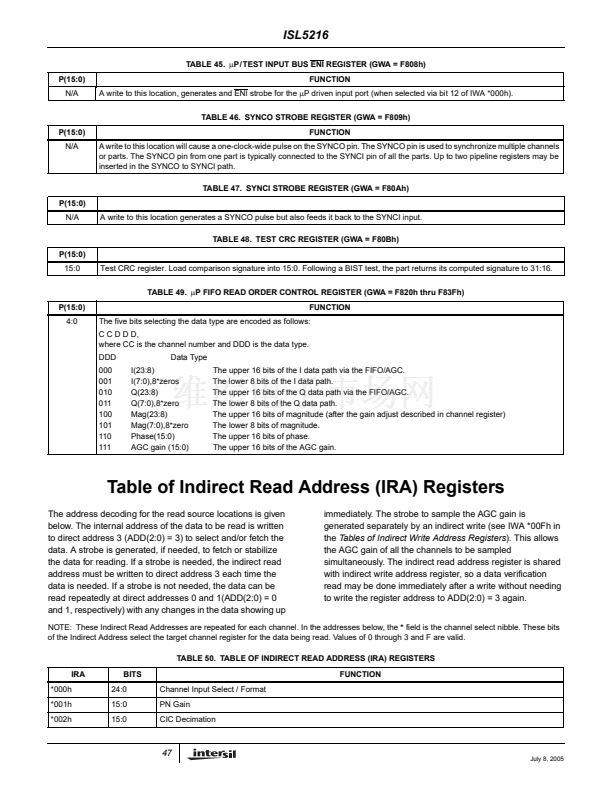
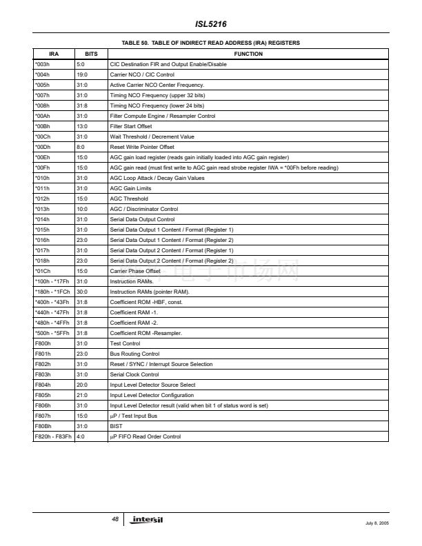
ISL5216
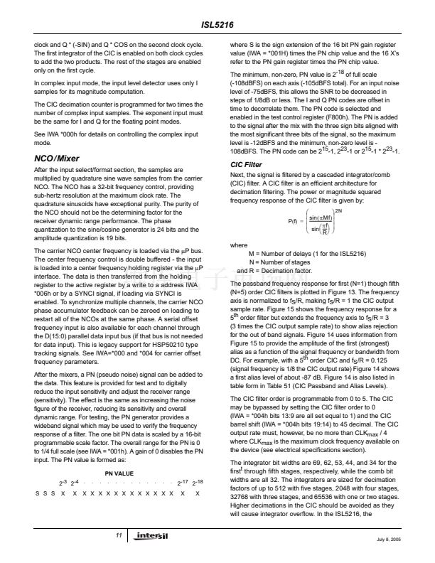
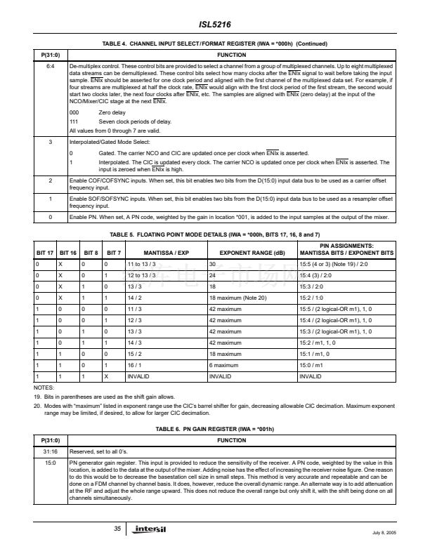
Serial Data Output Formatter Section
TO / FROM
OTHER CHANNELS
&
FIXED
TO
FLOAT
M
U
X
ROUND
&
SEQUENCER
1
DELAY
ZERO
PARALLEL
TO
SERIAL
&
& O
& R
&
SD2x
& O
& R
&
M
U
X
PARALLEL
TO
SERIAL
& O
& R
&
SD1x
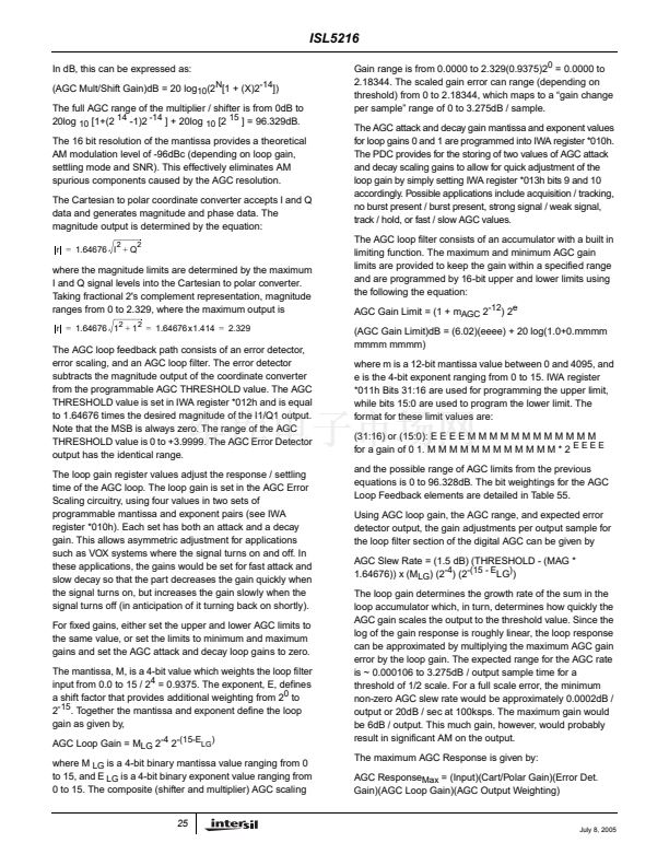
OUTPUT SECTION
ZERO
I1
Q1
MAG
PHASE
I2
Q2
GAIN
STROBE
R
E
G
SYNC
GEN
SYNCx
M
U
X
ROUND
SEQUENCER
2
M
U
X
16
TO
碌P
INTERFACE
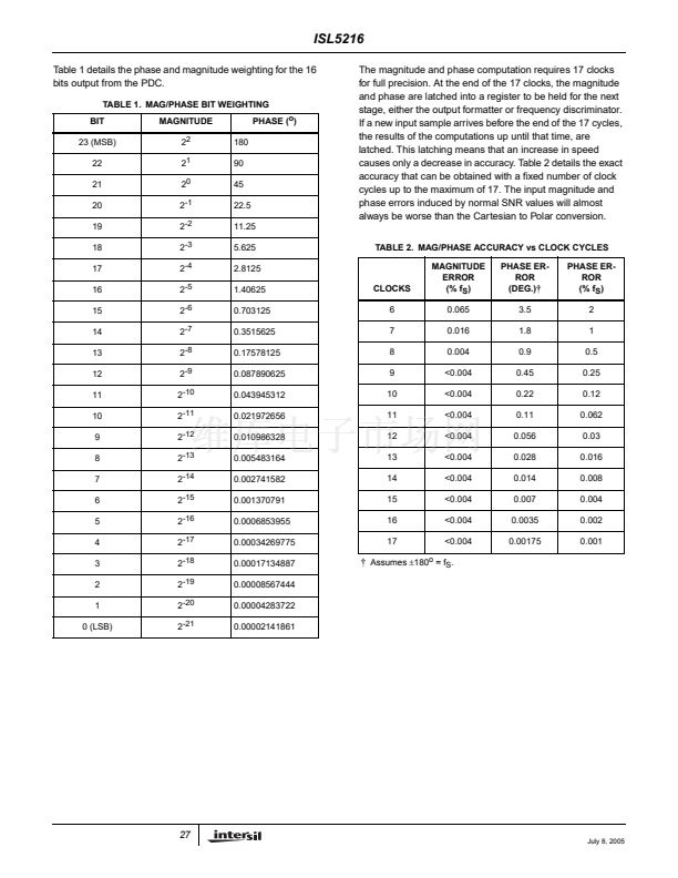
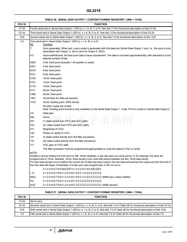
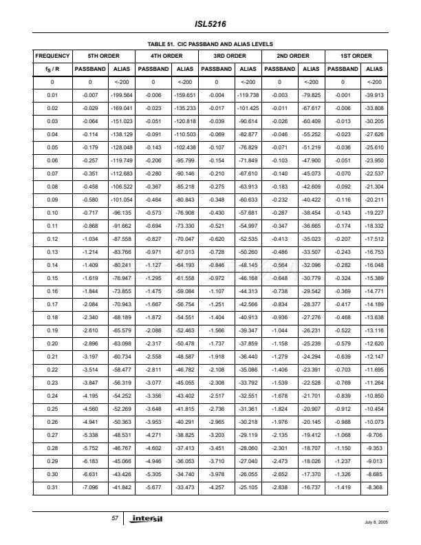
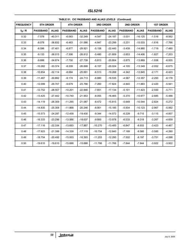
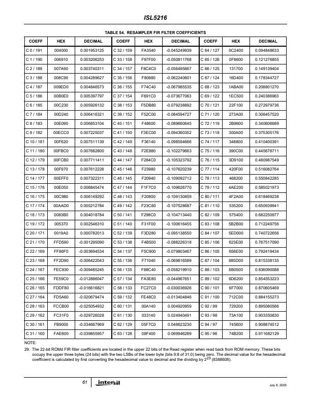
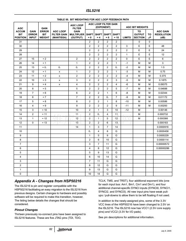
NOTE: Each serial output has 7 time slots. Each slot can contain I1, Q1, I2, Q2, Mag, phase or d蠁/dt, AGC gain, or zeros. Each slot can be 4, 6, 8,
10, 12, 16, 20, 24, or 32 (24 + 8 zeros) bits or disabled. Output 1 can also be 32-bit floating point. Slots can be disabled. A disabled slot will be one
clock wide if there are other active slots following. A sync can be asserted with any or all slots in output 1. The serial output can be delayed from 0
to 4095 serial clock periods from the input strobe. The serial outputs are always MSB first. The sync position applies to all time slots and can be one
clock prior to the first data bit, aligned with the first data bit, or one clock after the last data bit.
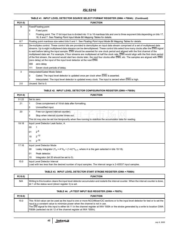
Serial Data Output Control Register
The serial data output control register contains sync position
and polarity (SYNCA, B, C or D), channel multiplexing, and
scaling controls for the SD1x and SD2x (x = A, B, C or D)
serial outputs (see Microprocessor Interface Section, IWA
register *014h).
Channel Routing Mask
The multiplexing mask bits for each channel (see
Microprocessor Interface Section, IWA register *014h bits
19:16 for SD1x or bits 15:12 for SD2x) can be used to enable
that channel鈥檚 output to any of the four serial outputs. These
bits control the AND gates that mask off the channels, so a
zero disables the channel鈥檚 connection to that output.
To configure more than one channel's output onto a serial
data output, the SD1 serial outputs and syncs from each
channel (0,1, 2 and 3) are brought to each of the SD1 serial
output sections and the SD2 serial outputs are brought to
28
each of the SD2 serial output sections (the syncs are only
associated with the SD1 serial outputs). There, the four
outputs are AND-ed with the multiplexing mask programmed
in the serial data output control registers of channels 0 thru 3
and OR-ed together. By gating off the channels that are not
wanted and delaying the data from each desired channel
appropriately, the channels can be multiplexed into a
common serial output stream. It should be noted that in
order to multiplex multiple channels onto a single serial data
stream the channels to be multiplexed must be synchronous.
Serial Data Output Time Slot Content/Format
Registers
These four registers are used to program the content and
format of the serial data output sequence time slots (see
Microprocessor Interface Section, IWA registers *015h -
*018h). There are seven data time slots that make up a serial
data output stream. The number of data bits and data format
July 8, 2005


 1
1
 2
2
 3
3
 4
4
 5
5
 6
6
 7
7
 8
8
 9
9
 10
10
 11
11
 12
12
 13
13
 14
14
 15
15
 16
16
 17
17
 18
18
 19
19
 20
20
 21
21
 22
22
 23
23
 24
24
 25
25
 26
26
 27
27
 28
28
 29
29
 30
30
 31
31
 32
32
 33
33
 34
34
 35
35
 36
36
 37
37
 38
38
 39
39
 40
40
 41
41
 42
42
 43
43
 44
44
 45
45
 46
46
 47
47
 48
48
 49
49
 50
50
 51
51
 52
52
 53
53
 54
54
 55
55
 56
56
 57
57
 58
58
 59
59
 60
60
 61
61
 62
62
 63
63
 64
64
 65
65
