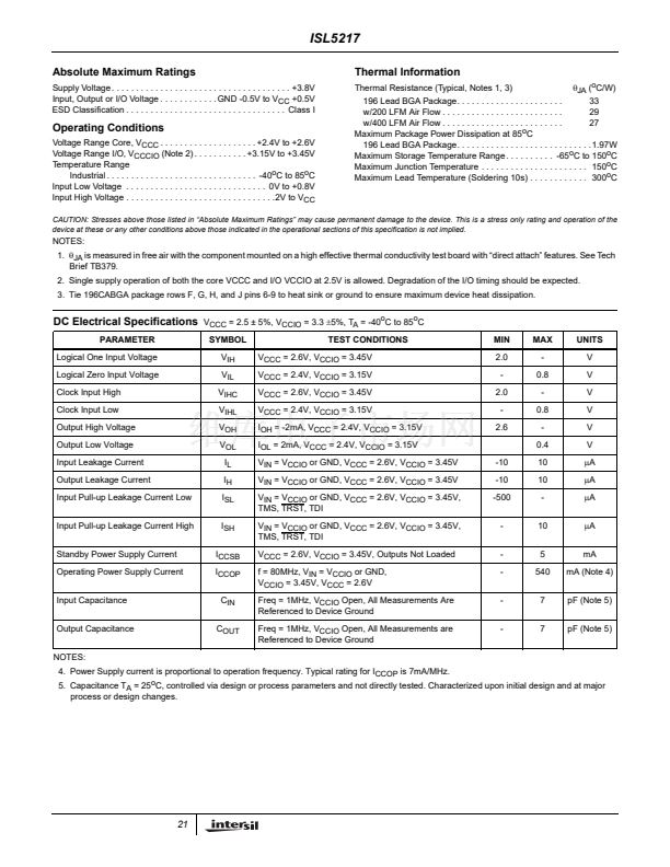
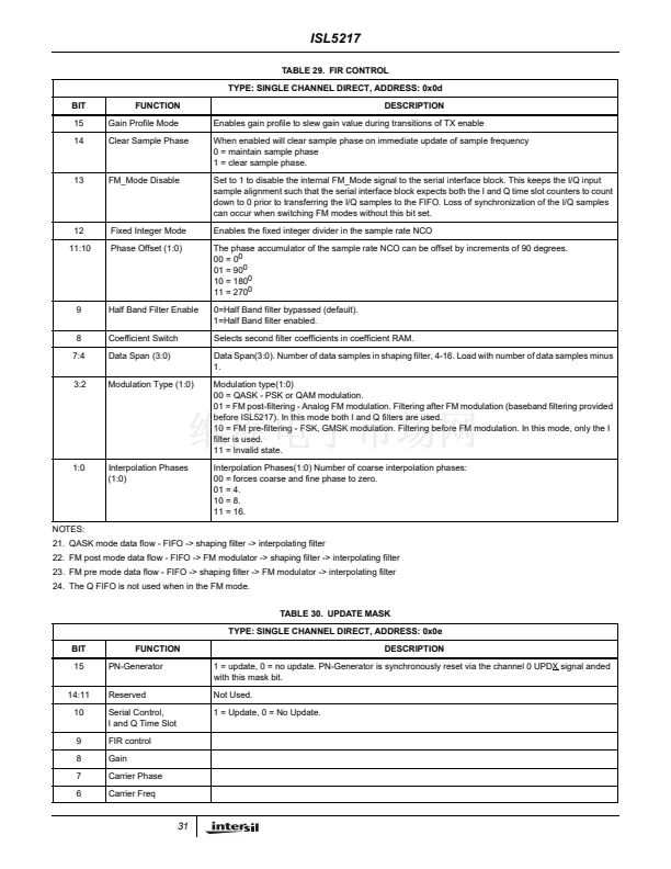
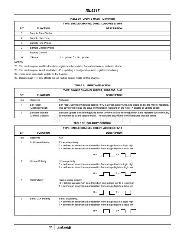
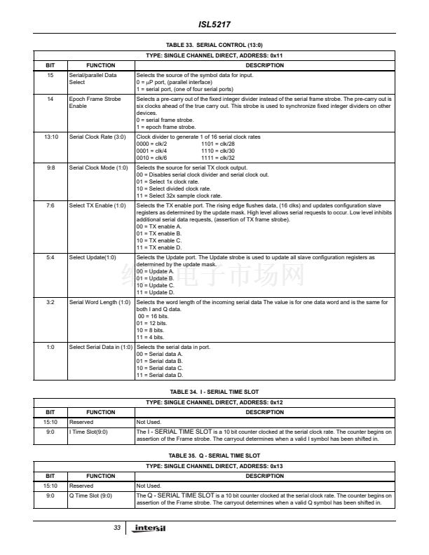
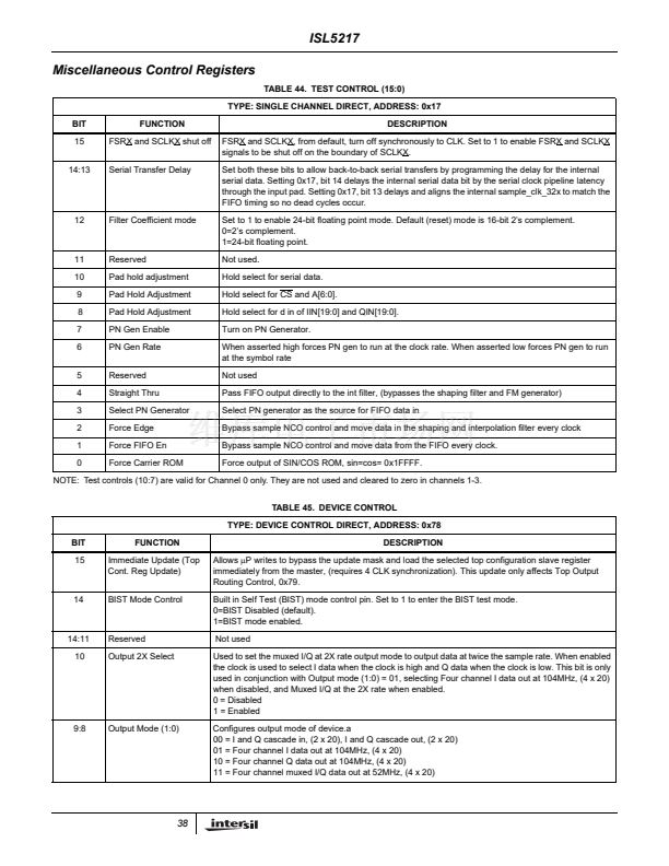
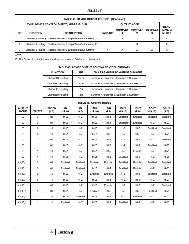
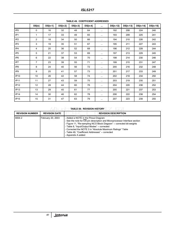
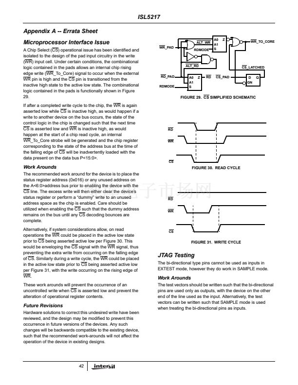
ISL5217
microprocessors can share a single QPUC as shown in
Figure 3.
SCLKX
MASTER
ISL5217
QPUC
SLAVE
ISL5217
QPUC
SLAVE
ISL5217
QPUC
SLAVE
ISL5217
QPUC
UPDX
SYNCO
碌P
UPDX
碌P
UPDX
碌P
UPDX
碌P
FSRX
SDX
SCLKX
FSRX
SDX
SCLKX
FSRX
SDX
SCLKX
FSRX
SDX
CHANNEL 3
CHANNEL 2
CHANNEL 1
ISL5217
QPUC
CHANNEL 0
SCLKX
碌P
FSRX
SDX
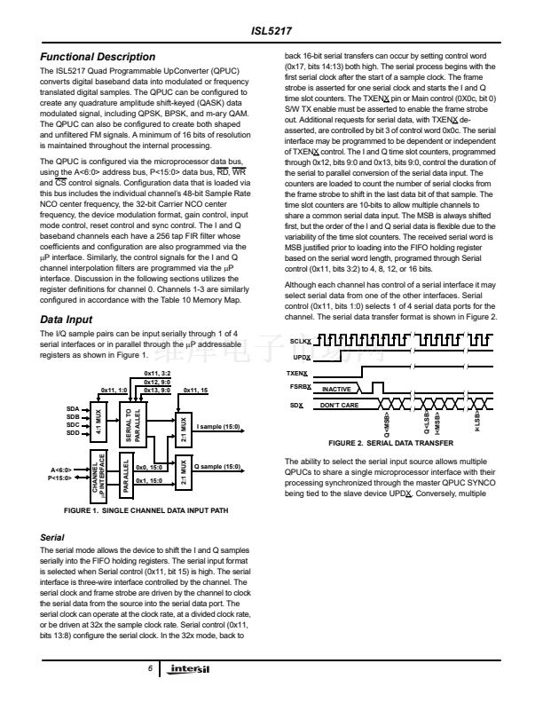
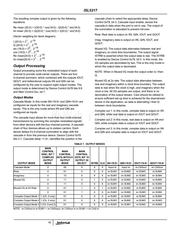
The input source to the FIFO is selected by Serial control
(15). The FIFO pointer is incremented every time data is
written into the FIFO. The transferring of data into the FIFO
does not occur until both I and Q have been received when
the sample data is input in a serial fashion. When the
sample data is input in a parallel fashion, the transferring of
data into the FIFO occurs when the
碌P
writes to Control
Word 0 (I data).
While the input source determines the write rate, the
shaping filter determines the read rate. The maximum read
rate occurs when the shaping filter constraints for Data
Span (DS) and Interpolation Phases (IP) equal four. For a
clock rate of 104MHz, the maximum read rate is
determined by f
CLK
/(DS)(IP), which is 104MHz/16 =
6.5MHz. See the Shaping Filter Section for more details.
When the Shaping Filter requires another data sample, a
request is made to the FIFO for data and the FIFO pointer
is decremented. Figure 5 indicates the timing of a request
for data from the Shaping filter to the actual appearance of
data at the FIFO output. An 鈥渆mpty鈥?FIFO detection causes
zero valued data to be entered into the shaping filter. The
FIFO can be forced to enter zero valued data by setting the
on-line mode to false. The on-line mode is enabled by Main
control (0xc, bit 6). A 鈥渇ull鈥?FIFO detection prevents data
from being pushed out of the FIFO before the filter requests
it. Writing to a full FIFO is treated as an error condition that
will result in a soft reset of the channel to prevent
transmission of erroneous data over the air. The full FIFO
channel reset can be disabled by control word 0x0c, bit 1.
A programmable FIFO depth threshold sets when the
FIFORDY signal is asserted, alerting the data source that
more data is required. The FIFORDY signal assists the
data source in maintaining the desired FIFO data depth.
The data FIFO depth threshold for both I and Q inputs is set
by Main control (0xc, bits 10:8). The SAMPLE CLK may be
used instead of FIFORDY to indicate when data has been
transferred from the FIFO to the shaping filter. See the pin
description table for additional details and Figure 5 for the
input data latency.
FIGURE 3. MULTIPLE CONFIGURATIONS
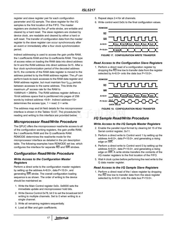
Parallel
The parallel mode allows the
碌P
to write the I and Q
samples directly to the FIFO holding registers. The parallel
input format is selected when Serial control (0x11, bit 15) is
low. The normal
碌P
write order is the Q sample, Control
word 0x1, followed by the I sample, Control word 0x0.
Writing to Control word 0x0 generates the update strobe to
move the data from the FIFO holding register into the first
location of the I/Q FIFO. The first location of the I/Q FIFO is
available for read back. The
碌P
can perform back-to-back
write accesses to Control words 0x1 and 0x0, but must
maintain four f
CLK
periods between accesses to the same
address. This limits the maximum
碌P
write access rate for
an I/ Q sample pair to 104MHz/4 = 26MHz. The Read/Write
format for a parallel data transfer is shown in Figure 4
CLK
RDMODE
RD
WR
A<6:0>
P<15:0>
01
Q
00
I
01
Q
00
I
01
Q
00
I
FIGURE 4. PARALLEL DATA TRANSFER
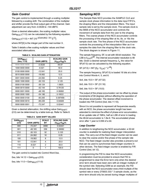
FIFO
The FIFO provides the interface and data storage between
the input source and the shaping filter or FM modulator. The
FIFO can hold up to seven I /Q sample pairs. The block
diagram is shown in Figure 6.
7


 1
1
 2
2
 3
3
 4
4
 5
5
 6
6
 7
7
 8
8
 9
9
 10
10
 11
11
 12
12
 13
13
 14
14
 15
15
 16
16
 17
17
 18
18
 19
19
 20
20
 21
21
 22
22
 23
23
 24
24
 25
25
 26
26
 27
27
 28
28
 29
29
 30
30
 31
31
 32
32
 33
33
 34
34
 35
35
 36
36
 37
37
 38
38
 39
39
 40
40
 41
41
 42
42
 43
43
