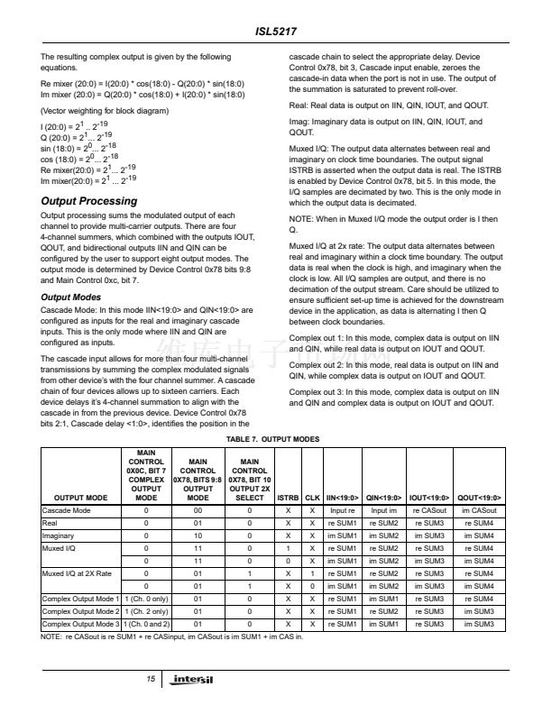
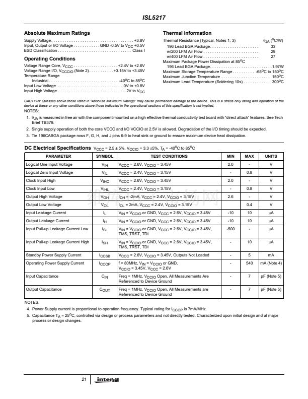
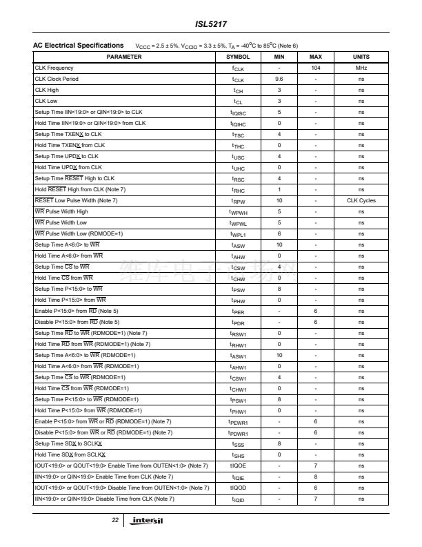
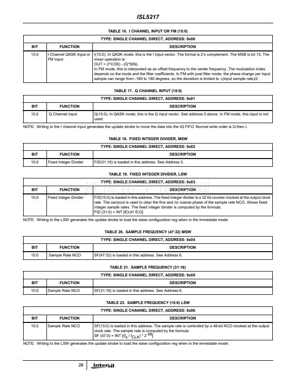
ISL5217
Appendix A -- Errata Sheet
Microprocessor Interface Issue
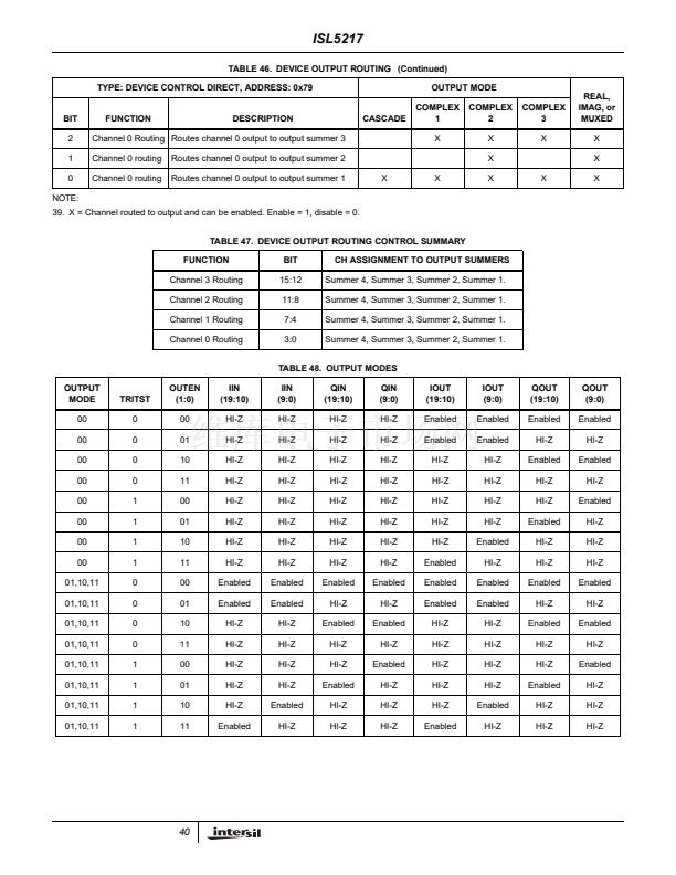
A Chip Select (CS) operational issue has been identified and
isolated to the design of the pad input circuitry in the write
(WR) input cell. Under certain conditions, the combinational
logic contained in the pads allows an internal chip rising
edge write (WR_To_Core) signal to occur when the external
WR pin is high and the CS pin is transitioned from the
inactive high state to the active low state. The combinational
logic contained in the pads is functionally shown in Figure
29.
If after a completed write cycle to the chip, the WR is again
asserted low while CS is inactive high, as would happen if a
write to another device on the bus occurs, the state of the
control logic in the chip is changed such that the next time
CS is asserted low and WR is inactive high, as would
happen at the start of a chip read cycle, an internal
WR_To_Core strobe will be generated and the chip register
corresponding to the state of the address bus at the time of
the falling edge of CS will be inadvertently loaded with the
data present on the data bus P<15:0>.
WR_PAD
ALT_WR
RDMODE
A0
A1
S
Z
WR_TO_CORE
ALT_RD
RD_PAD
RDMODE
RD
CS_PAD
CS_LATCHED
D
GN
Q
A0
A1
S
Z
FIGURE 29. CS SIMPLIFIED SCHEMATIC
RD
WR
CS
Work Arounds
The recommended work around for the device is to place the
status register address (0x016) or any unused address on
the A<6:0>address bus prior to enabling the device with the
CS line. The excess write will then either clear the device鈥檚
status register or perform a 鈥渄ummy鈥?write to an unused
address space as the chip is enabled. Care should be
utilized when enabling the CS such that the dummy address
remains on the bus until any CS decoding bounces are
complete.
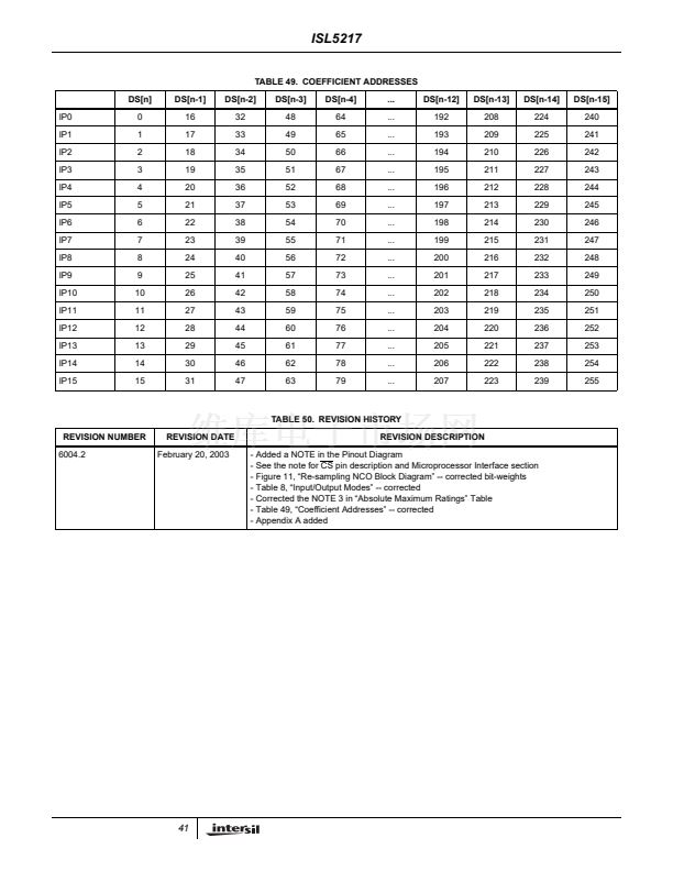
Alternatively, if system considerations allow, on read
operations the WR could be placed in the active low state
prior to CS being asserted active low per Figure 30. This
would be enveloping the CS signal with the WR signal, thus
preventing the extra write from occurring on the falling edge
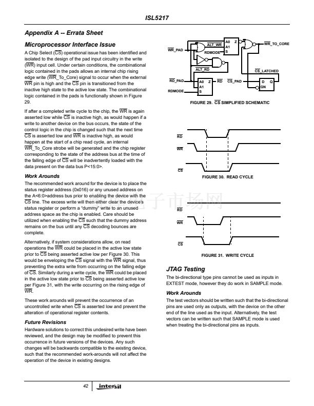
of CS. Similarly during a write cycle, the WR could be placed
in the active low state prior to CS being asserted active low
per Figure 31, with the write occurring on the rising edge of
WR.
These work arounds will prevent the occurrence of an
uncontrolled write when CS is asserted low and prevent the
alteration of operational register contents.
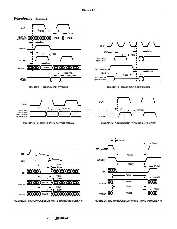
FIGURE 30. READ CYCLE
RD
WR
CS
FIGURE 31. WRITE CYCLE
JTAG Testing
The bi-directional type pins cannot be used as inputs in
EXTEST mode, however they do work in SAMPLE mode.
Work Arounds
The test vectors should be written such that the bi-directional
pins are used only as outputs, with the device on the other
end of the line used as the input. Alternatively, the test
vectors can be written such that SAMPLE mode is used
when treating the bi-directional pins as inputs.
Future Revisions
Hardware solutions to correct this undesired write have been
reviewed, and the design may be modified to prevent this
occurrence in future versions of the devices. Any such
changes will be backwards compatible to the existing device,
such that the recommended work-arounds will not affect the
operation of the device in existing designs.
42


 1
1
 2
2
 3
3
 4
4
 5
5
 6
6
 7
7
 8
8
 9
9
 10
10
 11
11
 12
12
 13
13
 14
14
 15
15
 16
16
 17
17
 18
18
 19
19
 20
20
 21
21
 22
22
 23
23
 24
24
 25
25
 26
26
 27
27
 28
28
 29
29
 30
30
 31
31
 32
32
 33
33
 34
34
 35
35
 36
36
 37
37
 38
38
 39
39
 40
40
 41
41
 42
42
 43
43
