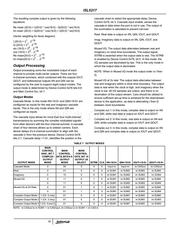
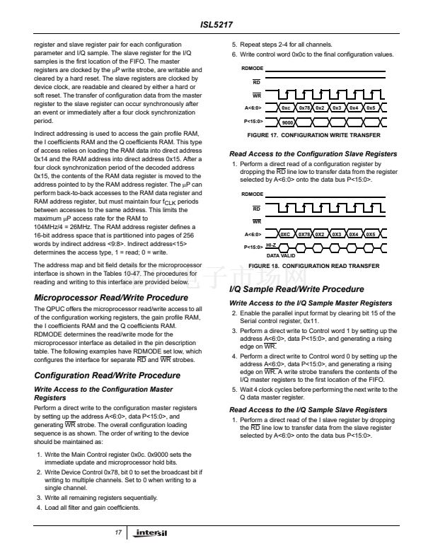
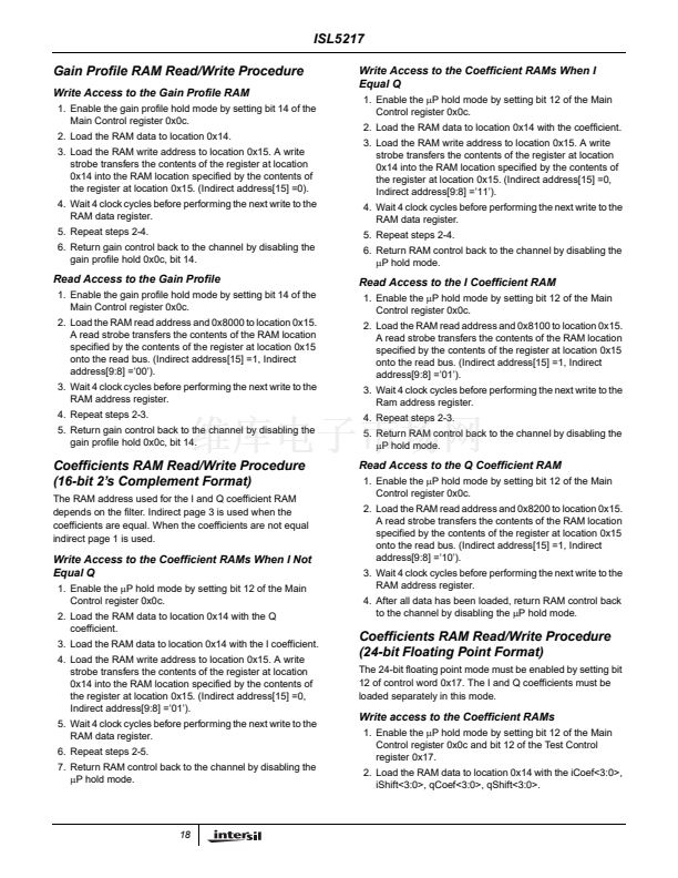
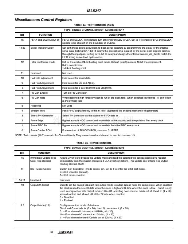
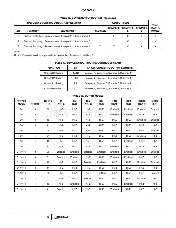
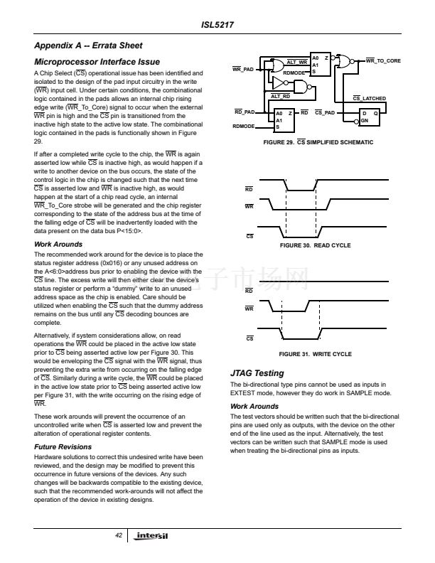
ISL5217
Gain Profile RAM Read/Write Procedure
Write Access to the Gain Profile RAM
1. Enable the gain profile hold mode by setting bit 14 of the
Main Control register 0x0c.
2. Load the RAM data to location 0x14.
3. Load the RAM write address to location 0x15. A write
strobe transfers the contents of the register at location
0x14 into the RAM location specified by the contents of
the register at location 0x15. (Indirect address[15] =0).
4. Wait 4 clock cycles before performing the next write to the
RAM data register.
5. Repeat steps 2-4.
6. Return gain control back to the channel by disabling the
gain profile hold 0x0c, bit 14.
Write Access to the Coefficient RAMs When I
Equal Q
1. Enable the
碌P
hold mode by setting bit 12 of the Main
Control register 0x0c.
2. Load the RAM data to location 0x14 with the coefficient.
3. Load the RAM write address to location 0x15. A write
strobe transfers the contents of the register at location
0x14 into the RAM location specified by the contents of
the register at location 0x15. (Indirect address[15] =0,
Indirect address[9:8] =鈥?1鈥?.
4. Wait 4 clock cycles before performing the next write to the
RAM data register.
5. Repeat steps 2-4.
6. Return RAM control back to the channel by disabling the
碌P
hold mode.
Read Access to the Gain Profile
1. Enable the gain profile hold mode by setting bit 14 of the
Main Control register 0x0c.
2. Load the RAM read address and 0x8000 to location 0x15.
A read strobe transfers the contents of the RAM location
specified by the contents of the register at location 0x15
onto the read bus. (Indirect address[15] =1, Indirect
address[9:8] =鈥?0鈥?.
3. Wait 4 clock cycles before performing the next write to the
RAM address register.
4. Repeat steps 2-3.
5. Return gain control back to the channel by disabling the
gain profile hold 0x0c, bit 14.
Read Access to the I Coefficient RAM
1. Enable the
碌P
hold mode by setting bit 12 of the Main
Control register 0x0c.
2. Load the RAM read address and 0x8100 to location 0x15.
A read strobe transfers the contents of the RAM location
specified by the contents of the register at location 0x15
onto the read bus. (Indirect address[15] =1, Indirect
address[9:8] =鈥?1鈥?.
3. Wait 4 clock cycles before performing the next write to the
Ram address register.
4. Repeat steps 2-3.
5. Return RAM control back to the channel by disabling the
碌P
hold mode.
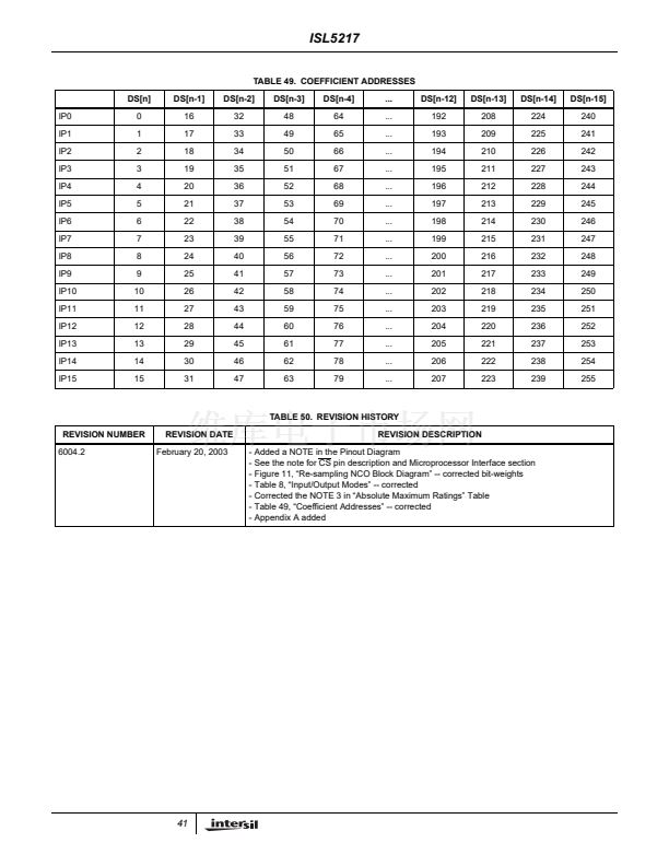
Coefficients RAM Read/Write Procedure
(16-bit 2鈥檚 Complement Format)
The RAM address used for the I and Q coefficient RAM
depends on the filter. Indirect page 3 is used when the
coefficients are equal. When the coefficients are not equal
indirect page 1 is used.
Read Access to the Q Coefficient RAM
1. Enable the
碌P
hold mode by setting bit 12 of the Main
Control register 0x0c.
2. Load the RAM read address and 0x8200 to location 0x15.
A read strobe transfers the contents of the RAM location
specified by the contents of the register at location 0x15
onto the read bus. (Indirect address[15] =1, Indirect
address[9:8] =鈥?0鈥?.
3. Wait 4 clock cycles before performing the next write to the
RAM address register.
4. After all data has been loaded, return RAM control back
to the channel by disabling the
碌P
hold mode.
Write Access to the Coefficient RAMs When I Not
Equal Q
1. Enable the
碌P
hold mode by setting bit 12 of the Main
Control register 0x0c.
2. Load the RAM data to location 0x14 with the Q
coefficient.
3. Load the RAM data to location 0x14 with the I coefficient.
4. Load the RAM write address to location 0x15. A write
strobe transfers the contents of the register at location
0x14 into the RAM location specified by the contents of
the register at location 0x15. (Indirect address[15] =0,
Indirect address[9:8] =鈥?1鈥?.
5. Wait 4 clock cycles before performing the next write to the
RAM data register.
6. Repeat steps 2-5.
7. Return RAM control back to the channel by disabling the
碌P
hold mode.
Coefficients RAM Read/Write Procedure
(24-bit Floating Point Format)
The 24-bit floating point mode must be enabled by setting bit
12 of control word 0x17. The I and Q coefficients must be
loaded separately in this mode.
Write access to the Coefficient RAMs
1. Enable the
碌P
hold mode by setting bit 12 of the Main
Control register 0x0c and bit 12 of the Test Control
register 0x17.
2. Load the RAM data to location 0x14 with the iCoef<3:0>,
iShift<3:0>, qCoef<3:0>, qShift<3:0>.
18


 1
1
 2
2
 3
3
 4
4
 5
5
 6
6
 7
7
 8
8
 9
9
 10
10
 11
11
 12
12
 13
13
 14
14
 15
15
 16
16
 17
17
 18
18
 19
19
 20
20
 21
21
 22
22
 23
23
 24
24
 25
25
 26
26
 27
27
 28
28
 29
29
 30
30
 31
31
 32
32
 33
33
 34
34
 35
35
 36
36
 37
37
 38
38
 39
39
 40
40
 41
41
 42
42
 43
43
