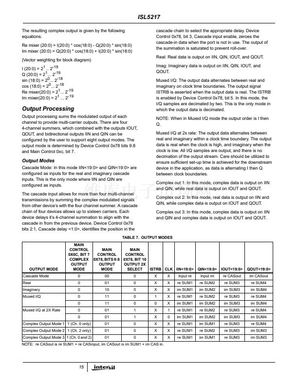
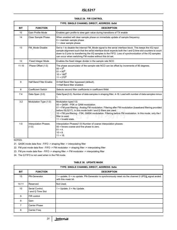
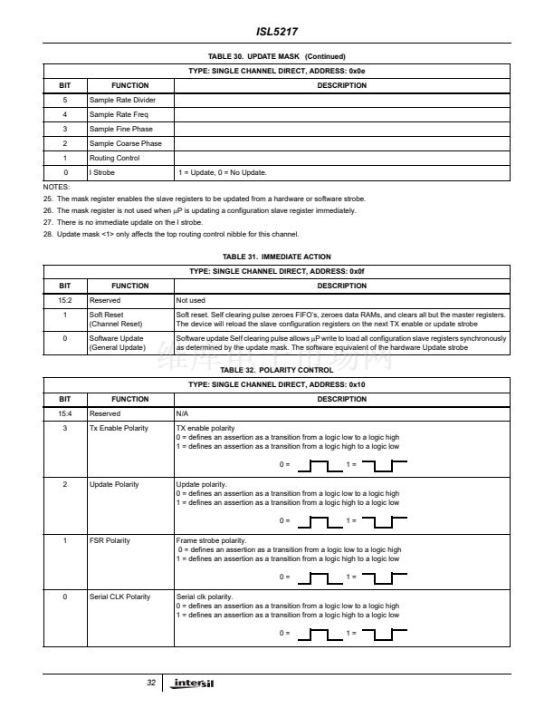
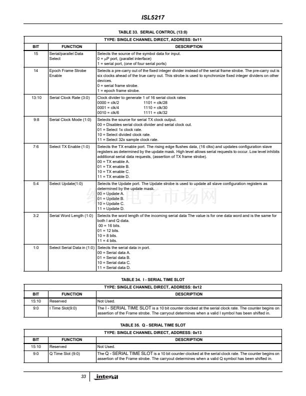
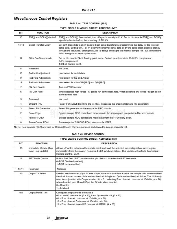
ISL5217
Polyphase output 1 = (D1*D[n]) + (D5*D[n-1]) + (D9*D[n-2])
+ (D13*D[n-3])
Polyphase output 2 = (D2*D[n]) + (D6*D[n-1]) + (D10*D[n-2])
+ (D14*D[n-3])
Polyphase output 3 = (D3*D[n]) + (D7*D[n-1]) + (D11*D[n-2])
+ (D15*D[n-3])
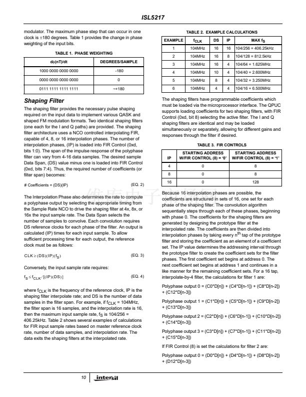
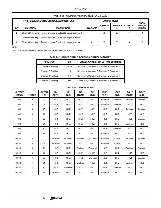
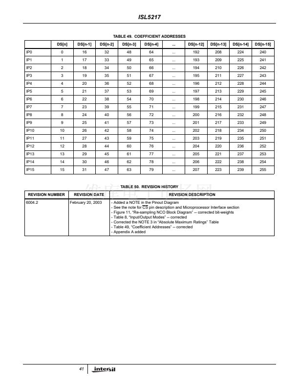
Table 4 details the coefficient address allocation for the
previous example. The interpolation phase is on the left and
the data span is across the top. The coefficient RAM address
followed by the coefficient term is listed in the table鈥檚 cell.
Table 49 details the coefficient address locations through
255.
TABLE 4. ADDRESS ALLOCATION
DS [n]
IP0
IP1
IP2
IP3
IP4
IP5
IP6
IP7
IP8
IP9
IP10
IP11
IP12
IP13
IP14
IP15
DS [n-1]
DS [n-2]
DS [n-3]
The gain through the filter is:
A = (sum of coefficients) / interpolation rate.
The shaping filter contains saturation logic in the event that
the final output peaks over +/- 1.0. When using quadrature
modulation, saturation/overflow can occur when the input
values for I and Q exceed 0.707 peak. The shaping filter
coefficients may need to be reduced from full scale to
prevent saturation.
Gain Profile
The overall channel gain is controlled by both a gain profile
stage and a gain control stage, which provide identical scaling
for the I and Q upconverted data. The gain profile stage allows
transmit ramp-up and quench fading, to control the sidelobe
profile in burst mode. This is implemented through user control
of the rise and fall transitions utilizing a gain profile memory.
The gain profile memory is a 128 x 12 bit RAM which is loaded
with the desired scaling coefficients via indirect addressing of
memory spaces 0x000-0x07f. The pulse shaping is
implemented by linearly multiplying the programmed coefficient
by the shaping filter outputs at the f
S
*IP or coarse phase rate.
,
The gain profile is enabled by FIR control (0xd, bit 15), with the
RAM address pointer being reset to zero on assertion of the
gain profile enable. Control of the pulse shaping is based on
TXENX, as the TXENX rising edge causes the RAM pointer to
begin stepping through the profile until the RAM pointer
matches the Gain profile length programed into control word
(0x0b, bits 6:0). The falling edge of TXENX reverses the
process and the RAM pointer begins decrementing until it
reaches zero. The gain process is symmetric with respect to the
rising or falling edges of TXENX. The latency through the gain
profile block is set by control word (0x0b, bits 8:7) where bit 8
bypasses all latency alignment circuitry and uses TXENX as
input to the channel. Setting control word (0x0b, bit 7) removes
two edge latencies from the delay path and should be
combined with selection of DS = 3, IP = 4 in order to have
perfect symmetry through the gain profile block. The memory
coefficients may be loaded without taking the channel off-line.
This is implemented by setting the gain profile hold bit in control
word (0x0c, bit 14) which holds the last gain value and provides
access to the memory.
The gain profile coefficients are programmed as unsigned
values:
Bit weight 2
0
.2
-1
2
-2
... 2
-11
Maximum 0x800 = 1.0
0x001 = 2
-11
Minimum
0x000 = 0.0
0
1
2
3
4
5
6
7
8
9
CO
C1
C2
C3
16 C4
17 C5
18 C6
19 C7
20
21
22
23
32 C8
33 C9
34 C10
35 C11
36
37
38
39
40 D8
41 D9
42 D10
43 D11
44
45
46
47
48 C12
49 C13
50 C14
51 C15
52
53
54
55
56 D12
57 D13
58 D14
59 D15
60
61
62
63
鈥?/div>
鈥?/div>
鈥?/div>
鈥?/div>
鈥?/div>
鈥?/div>
鈥?/div>
鈥?/div>
鈥?/div>
鈥?/div>
鈥?/div>
鈥?/div>
鈥?/div>
鈥?/div>
鈥?/div>
鈥?/div>
D0
D1
24 D4
25 D5
26 D6
27 D7
28
29
30
31
10 D2
11 D3
12
13
14
15
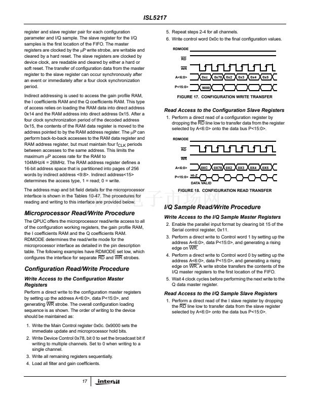
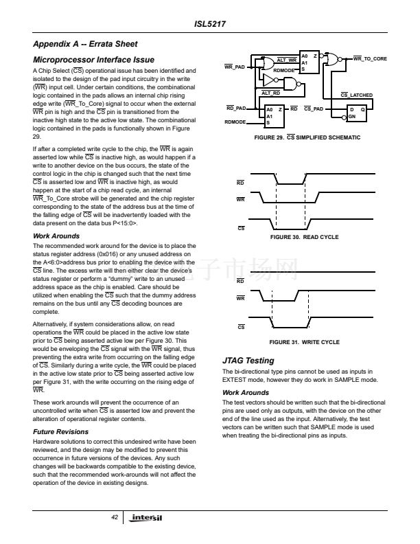
The loading options are programmable including read back
modes and are discussed in detail in the 鈥楳icroprocessor
Interface鈥?section. Both 16-bit 2鈥檚 complement and 24-bit
floating point format are allowed. The 2鈥檚 complement
coefficient format of valid digital values ranges from 0x8001
to 0x7FFF. The value 8000 is not allowed. The 24-bit floating
point (20-bit mantissa with 4-bit exponent) mode allows an
exponent range from 0 to 15. An exponent of 0 indicates
multiplication of the coefficient by 2
0
, and an exponent of 1 is
2
-1
, down to a value of 15 being 2
-15
. The default mode is 2鈥檚
complement, with 24-bit floating point mode enabled by
setting control word (0x17, bit 12).
11
ISL5217 PDF文件相關(guān)型號(hào)
ISL5217KIZ
ISL5217相關(guān)型號(hào)PDF文件下載
-
型號(hào)
版本
描述
廠商
下載
-
英文版
Low-Voltage, Single Supply, Dual SPST, SPDT Analog Switches
-
英文版
Low-Voltage, Single Supply, Dual SPST, SPDT Analog Switches
INTERSIL [...
-
英文版
Low-Voltage, Single Supply, Dual SPST, SPDT Analog Switches
-
英文版
Low-Voltage, Single Supply, Dual SPST, SPDT Analog Switches
INTERSIL [...
-
英文版
Low-Voltage, Single Supply, Dual SPST, SPDT Analog Switches
-
英文版
Low-Voltage, Single Supply, Dual SPST, SPDT Analog Switches
-
英文版
Four-Channel Programmable Digital DownConverter
-
英文版
Quad Programmable Up Converter
-
英文版
Pre-Distortion Linearizer
-
英文版
CommLink Direct Digital Synthesizer
-
英文版
Four-Channel Wideband Programmable DownConverter
-
英文版
3.3V Ringing SLIC Family for Voice Over Broadband (VOB)
-
英文版
Low Power Ringing SLIC for Home Gateways
-
英文版
Dual 8-bit, +3.3V, 260+MSPS, High Speed D/A Converter
-
英文版
Dual 8-bit, +3.3V, 130/210+MSPS, High Speed D/A Converter
-
英文版
3V Dual 8-Bit, 20/40/60MSPS A/D Converter with Internal Volt...
-
英文版
Dual 10-bit, +3.3V, 260+MSPS, High Speed D/A Converter
-
英文版
Dual 10-bit, +3.3V, 130/210+MSPS, High Speed D/A Converter
-
英文版
3V Dual 10-Bit, 20/40/60MSPS A/D Converter with Internal Vol...
-
英文版
10-bit, +3.3V, 260+MSPS, High Speed D/A Converter


 1
1
 2
2
 3
3
 4
4
 5
5
 6
6
 7
7
 8
8
 9
9
 10
10
 11
11
 12
12
 13
13
 14
14
 15
15
 16
16
 17
17
 18
18
 19
19
 20
20
 21
21
 22
22
 23
23
 24
24
 25
25
 26
26
 27
27
 28
28
 29
29
 30
30
 31
31
 32
32
 33
33
 34
34
 35
35
 36
36
 37
37
 38
38
 39
39
 40
40
 41
41
 42
42
 43
43
