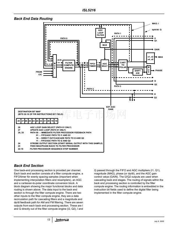
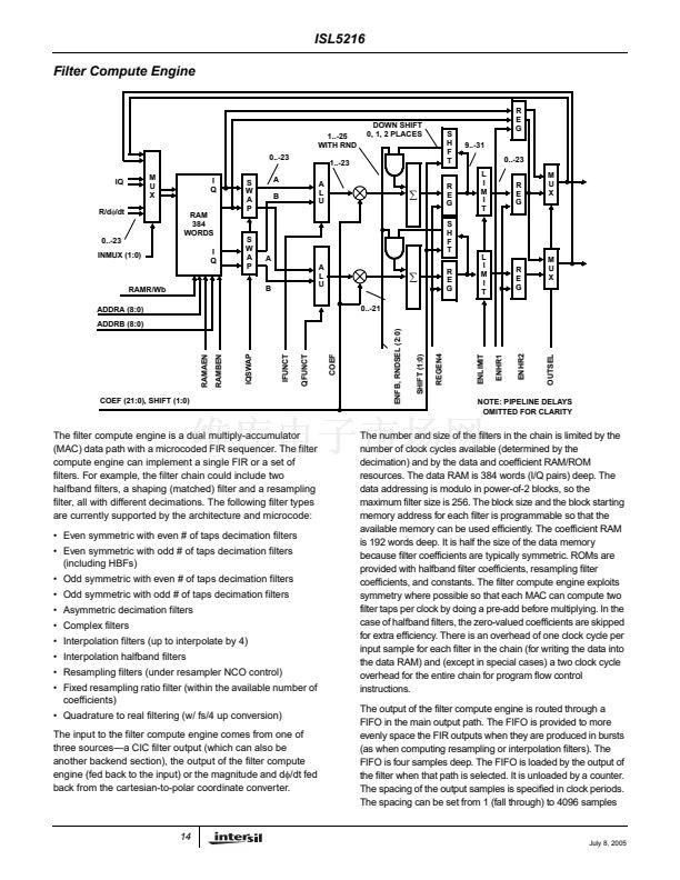
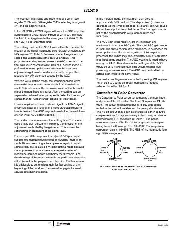
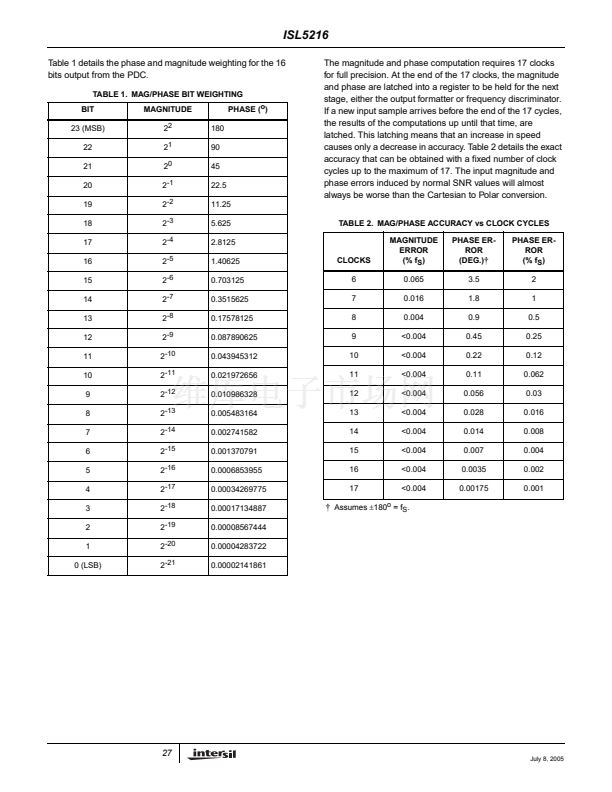
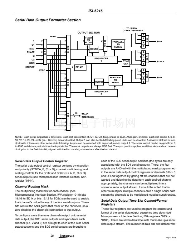
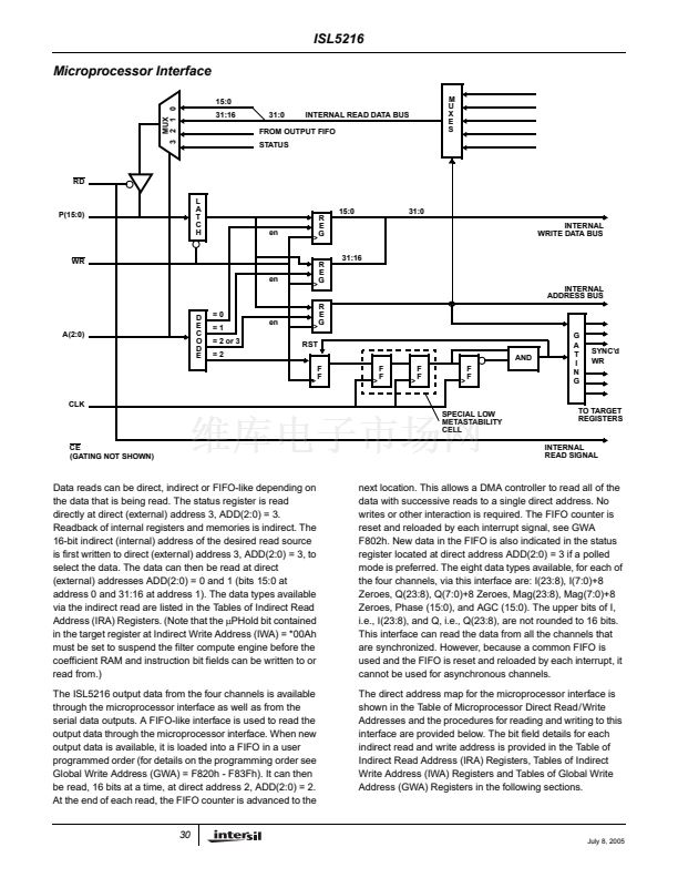
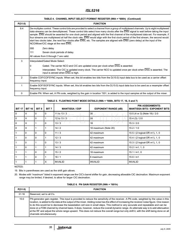
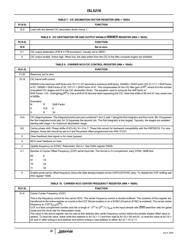
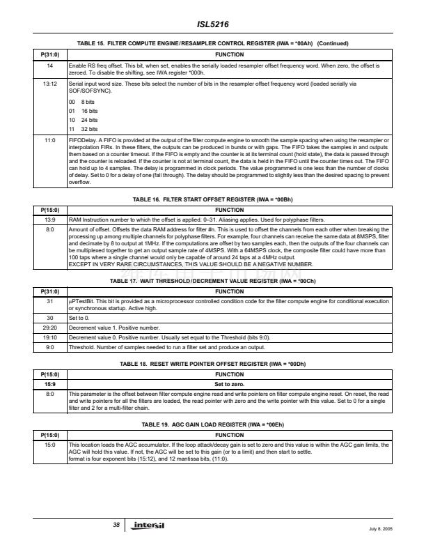
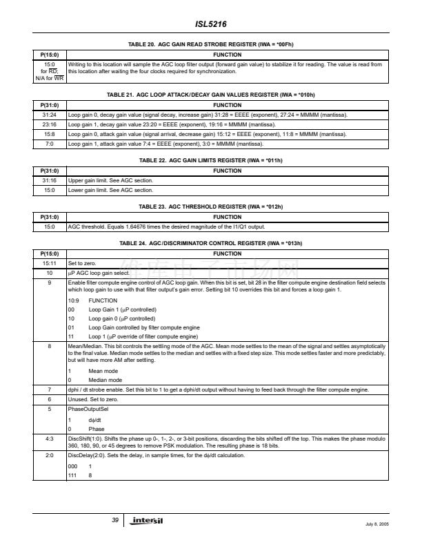
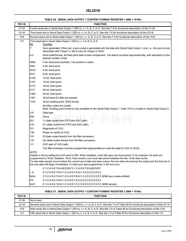
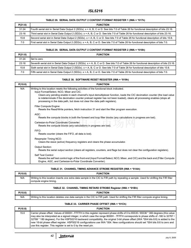
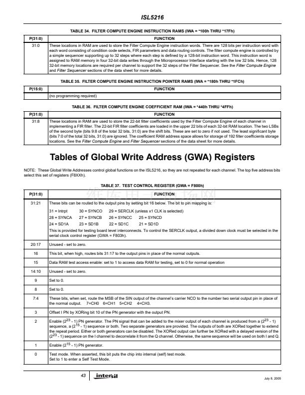
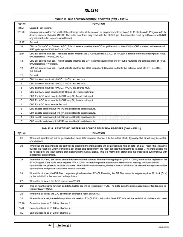
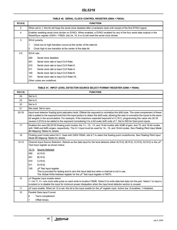
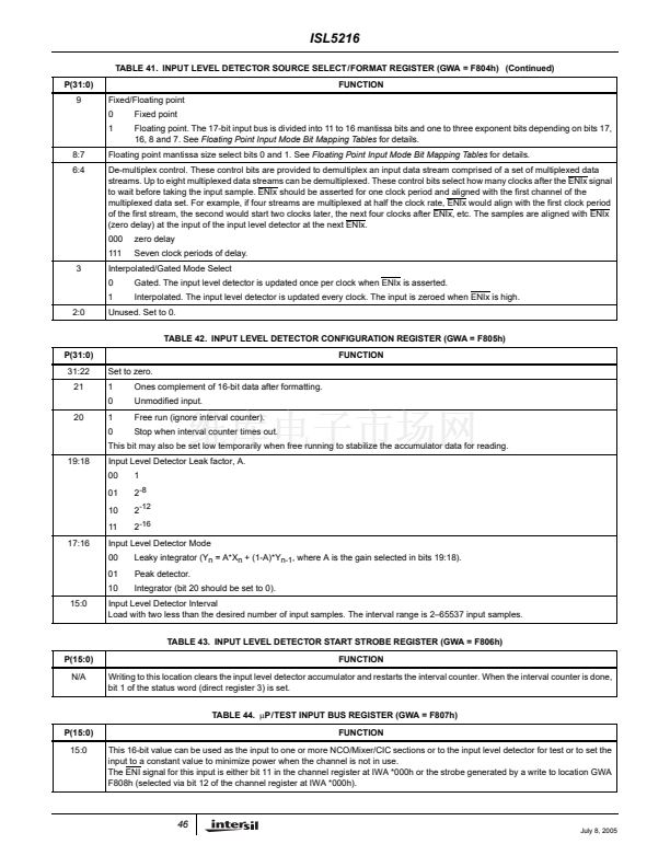
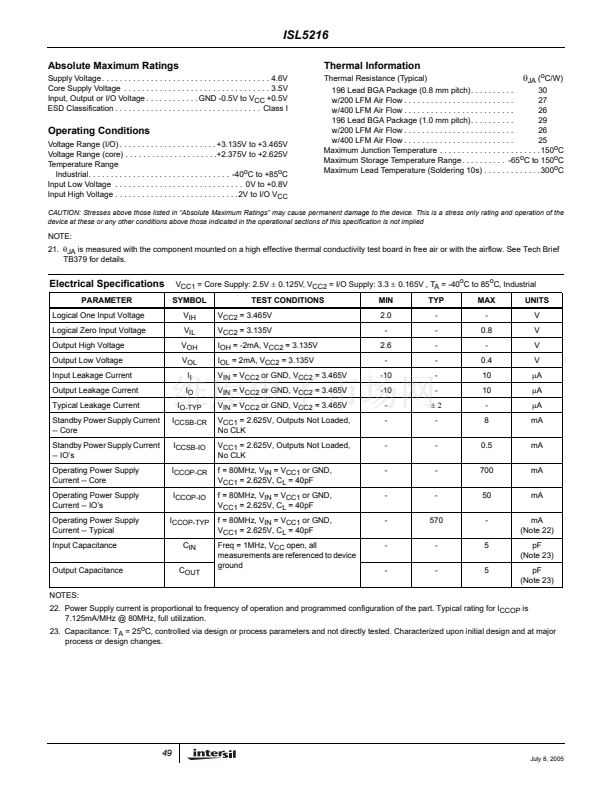
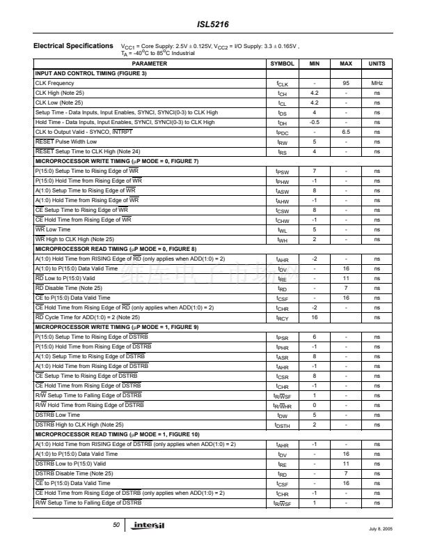
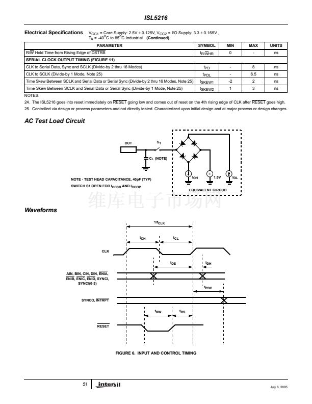
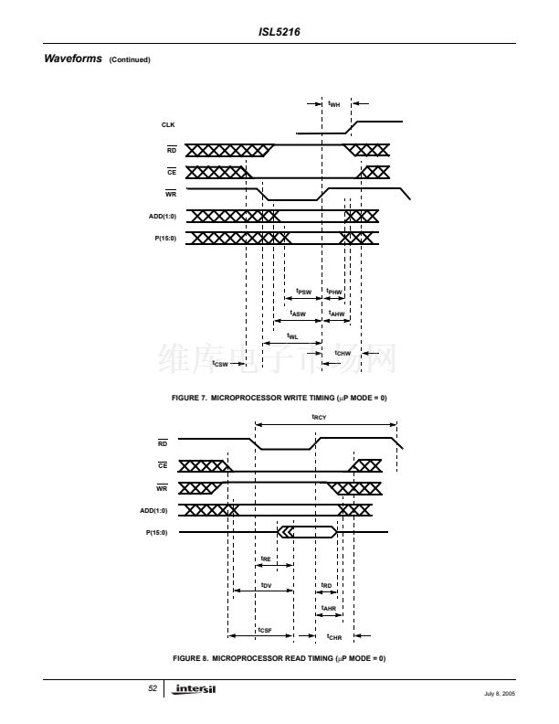
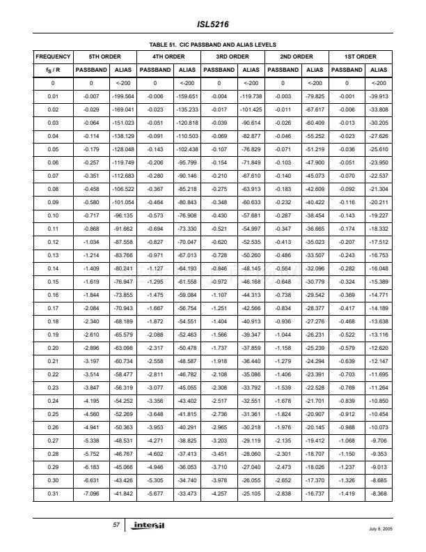
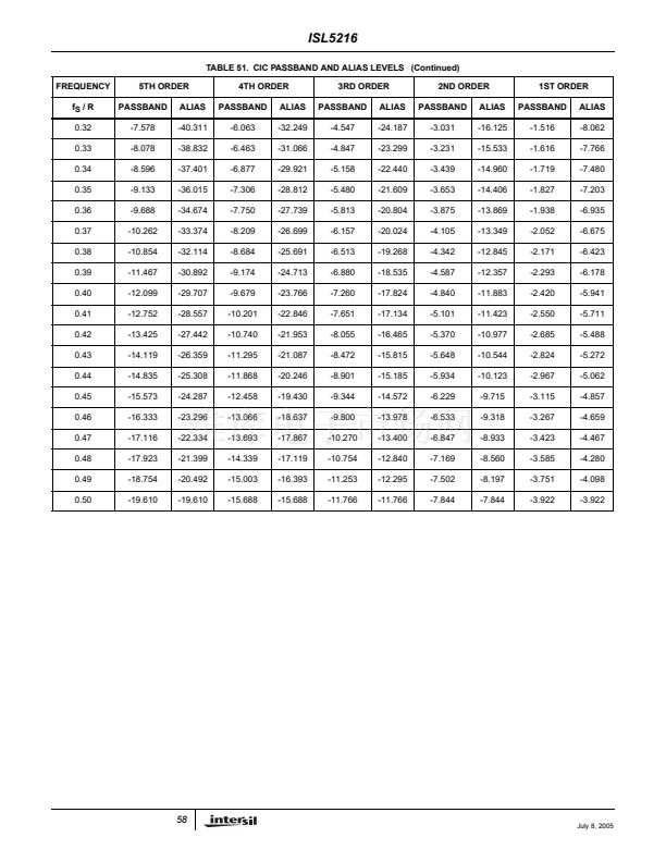
ISL5216
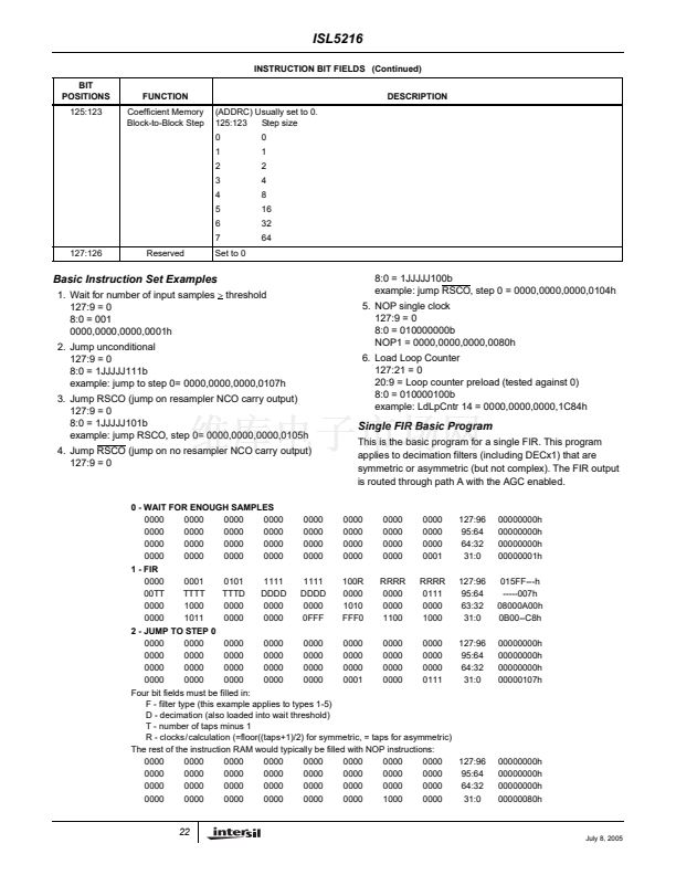
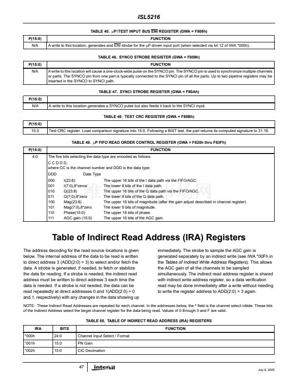
TABLE 45.
碌P/TEST
INPUT BUS ENI REGISTER (GWA = F808h)
P(15:0)
N/A
FUNCTION
A write to this location, generates and ENI strobe for the
碌P
driven input port (when selected via bit 12 of IWA *000h).
TABLE 46. SYNCO STROBE REGISTER (GWA = F809h)
P(15:0)
N/A
FUNCTION
A write to this location will cause a one-clock-wide pulse on the SYNCO pin. The SYNCO pin is used to synchronize multiple channels
or parts. The SYNCO pin from one part is typically connected to the SYNCI pin of all the parts. Up to two pipeline registers may be
inserted in the SYNCO to SYNCI path.
TABLE 47. SYNCI STROBE REGISTER (GWA = F80Ah)
P(15:0)
N/A
A write to this location generates a SYNCO pulse but also feeds it back to the SYNCI input.
TABLE 48. TEST CRC REGISTER (GWA = F80Bh)
P(15:0)
15:0
Test CRC register. Load comparison signature into 15:0. Following a BIST test, the part returns its computed signature to 31:16.
TABLE 49.
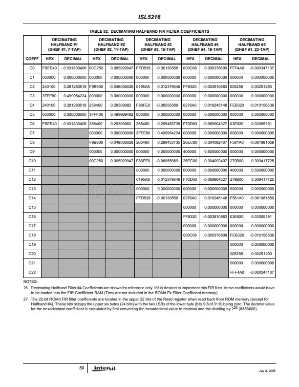
碌P
FIFO READ ORDER CONTROL REGISTER (GWA = F820h thru F83Fh)
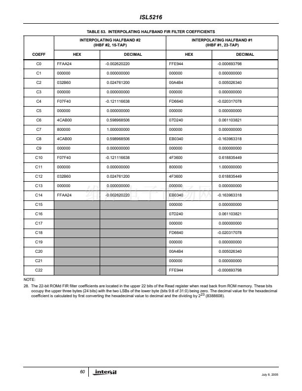
P(15:0)
4:0
C C D D D,
where CC is the channel number and DDD is the data type.
DDD
000
001
010
011
100
101
110
111
Data Type
I(23:8)
I(7:0),8*zeros
Q(23:8)
Q(7:0),8*zero
Mag(23:8)
Mag(7:0),8*zero
Phase(15:0)
AGC gain (15:0)
The upper 16 bits of the I data path via the FIFO/AGC.
The lower 8 bits of the I data path.
The upper 16 bits of the Q data path via the FIFO/AGC.
The lower 8 bits of the Q data path.
The upper 16 bits of magnitude (after the gain adjust described in channel register)
The lower 8 bits of magnitude.
The upper 16 bits of phase.
The upper 16 bits of the AGC gain.
FUNCTION
The five bits selecting the data type are encoded as follows:
Table of Indirect Read Address (IRA) Registers
The address decoding for the read source locations is given
below. The internal address of the data to be read is written
to direct address 3 (ADD(2:0) = 3) to select and/or fetch the
data. A strobe is generated, if needed, to fetch or stabilize
the data for reading. If a strobe is needed, the indirect read
address must be written to direct address 3 each time the
data is needed. If a strobe is not needed, the data can be
read repeatedly at direct addresses 0 and 1(ADD(2:0) = 0
and 1, respectively) with any changes in the data showing up
immediately. The strobe to sample the AGC gain is
generated separately by an indirect write (see IWA *00Fh in
the
Tables of Indirect Write Address Registers).
This allows
the AGC gain of all the channels to be sampled
simultaneously. The indirect read address register is shared
with indirect write address register, so a data verification
read may be done immediately after a write without needing
to write the register address to ADD(2:0) = 3 again.
NOTE: These Indirect Read Addresses are repeated for each channel. In the addresses below, the
*
field is the channel select nibble. These bits
of the Indirect Address select the target channel register for the data being read. Values of 0 through 3 and F are valid.
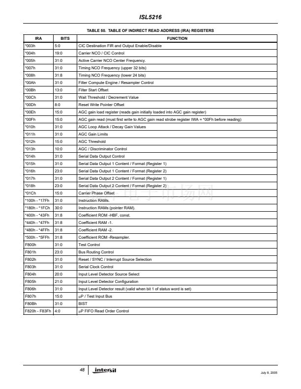
TABLE 50. TABLE OF INDIRECT READ ADDRESS (IRA) REGISTERS
IRA
*000h
*001h
*002h
BITS
24:0
15:0
15:0
Channel Input Select / Format
PN Gain
CIC Decimation
FUNCTION
47
July 8, 2005


 1
1
 2
2
 3
3
 4
4
 5
5
 6
6
 7
7
 8
8
 9
9
 10
10
 11
11
 12
12
 13
13
 14
14
 15
15
 16
16
 17
17
 18
18
 19
19
 20
20
 21
21
 22
22
 23
23
 24
24
 25
25
 26
26
 27
27
 28
28
 29
29
 30
30
 31
31
 32
32
 33
33
 34
34
 35
35
 36
36
 37
37
 38
38
 39
39
 40
40
 41
41
 42
42
 43
43
 44
44
 45
45
 46
46
 47
47
 48
48
 49
49
 50
50
 51
51
 52
52
 53
53
 54
54
 55
55
 56
56
 57
57
 58
58
 59
59
 60
60
 61
61
 62
62
 63
63
 64
64
 65
65
