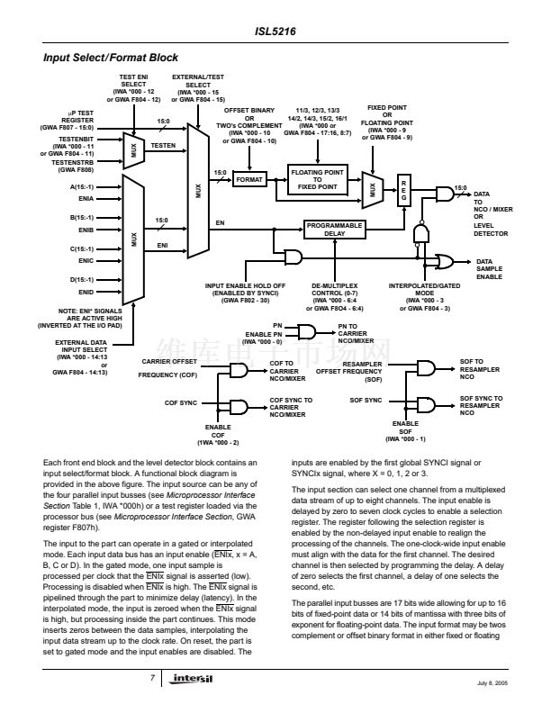
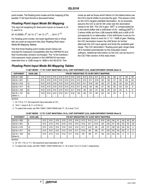
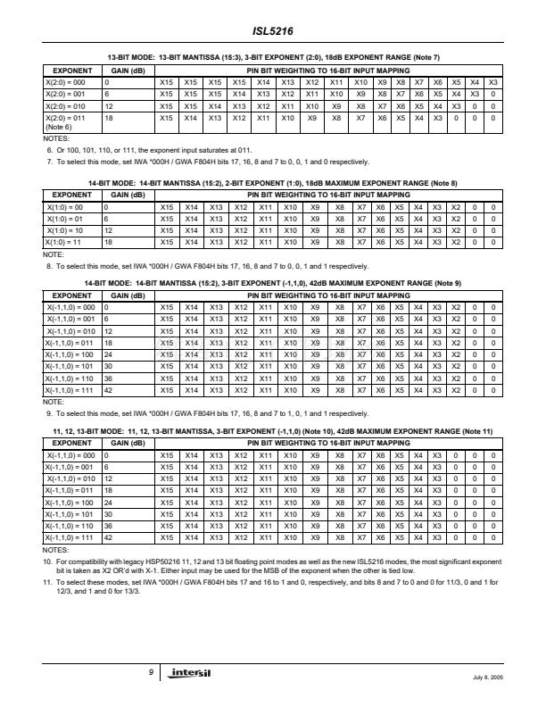
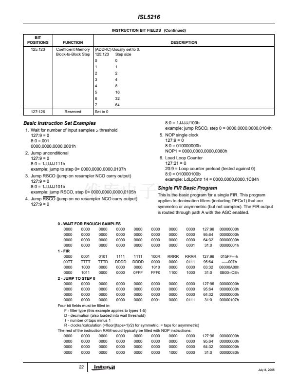
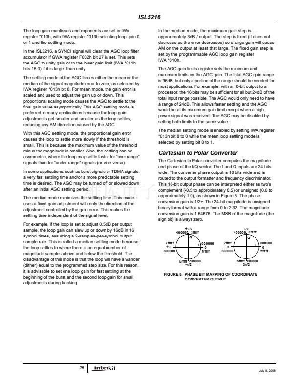
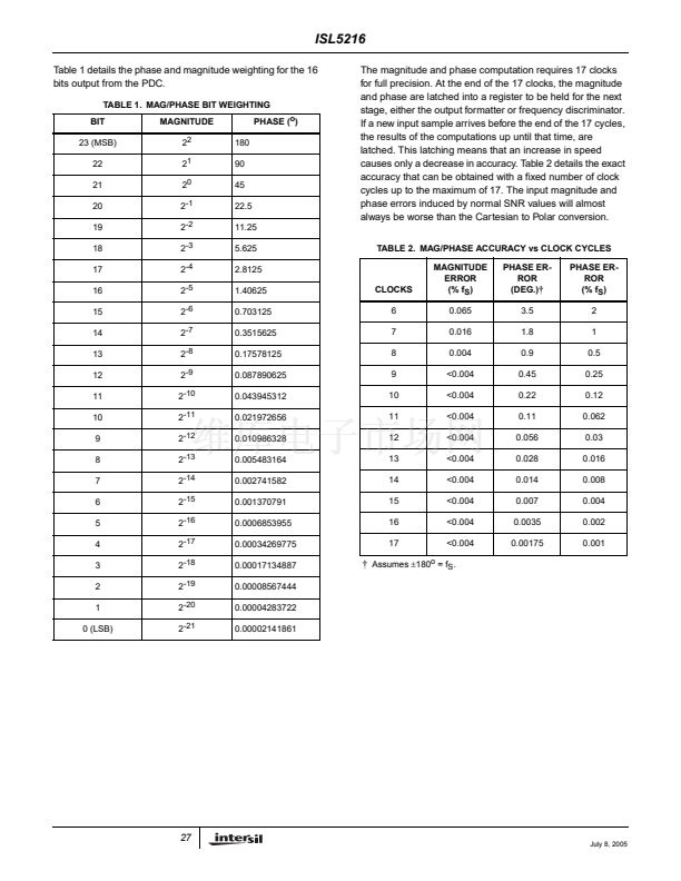
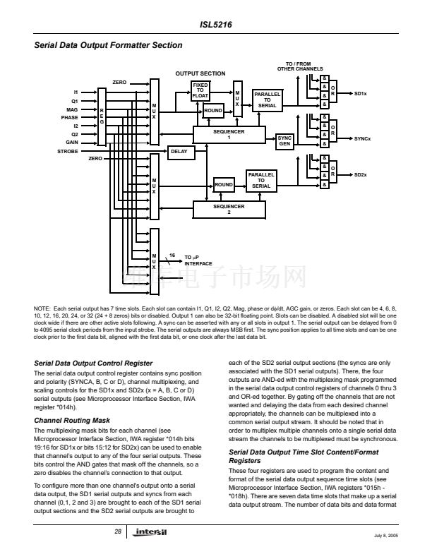
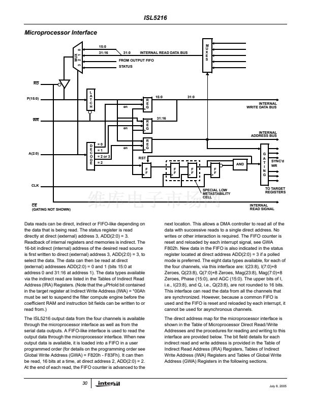
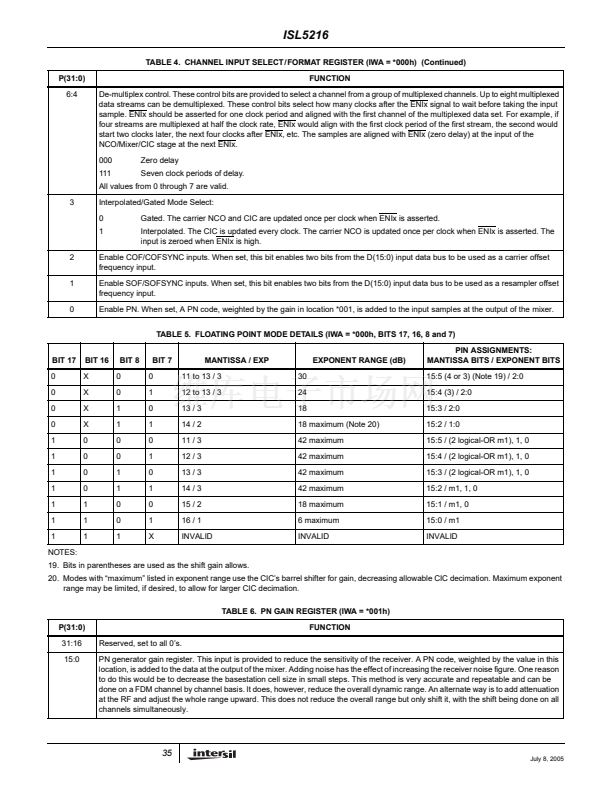
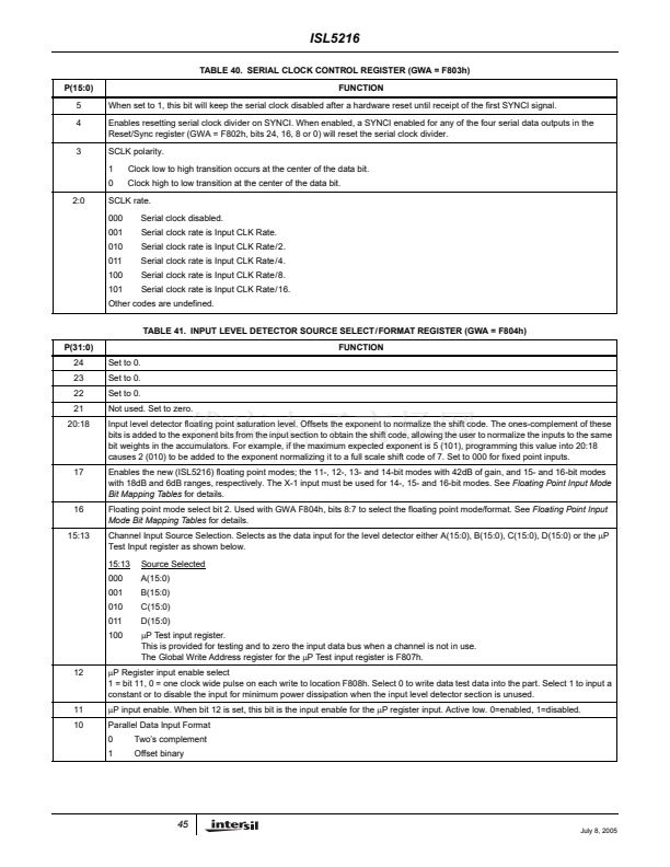
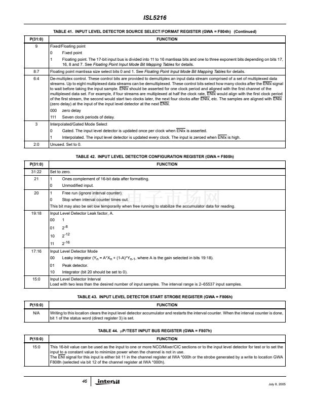
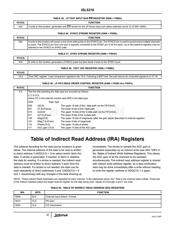
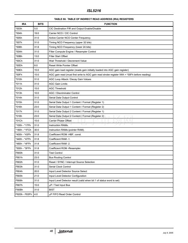
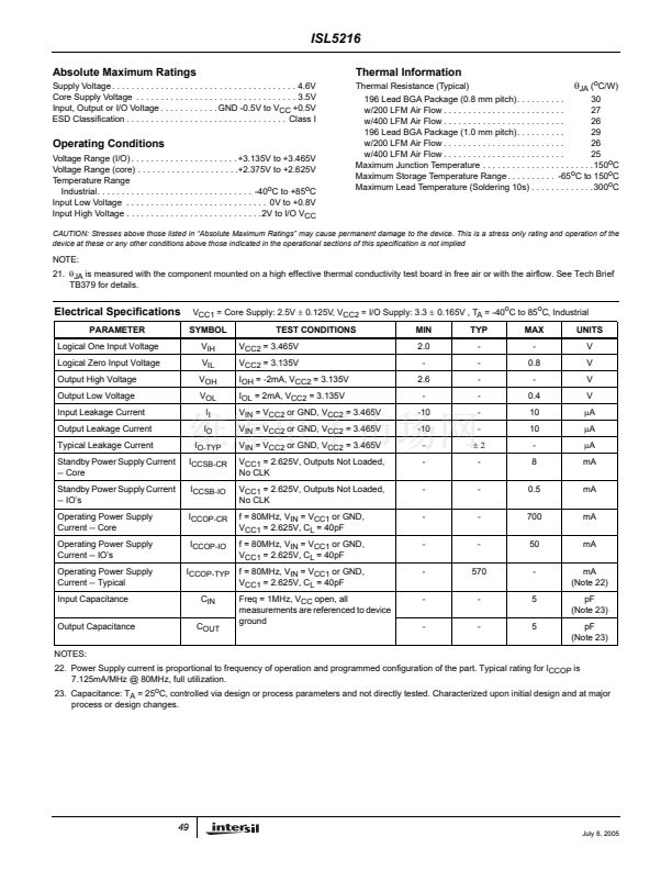
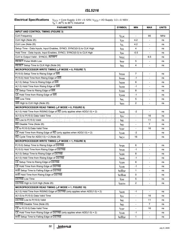
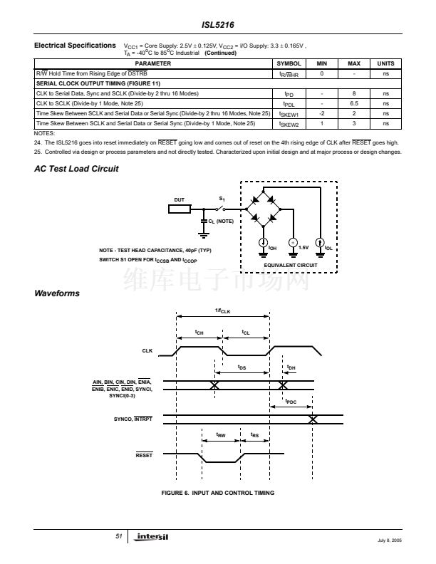
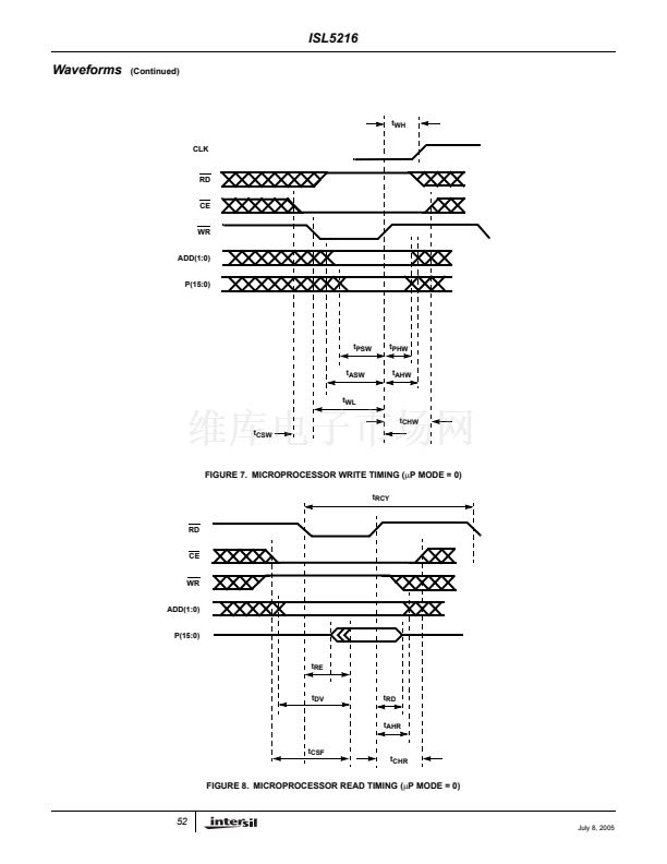
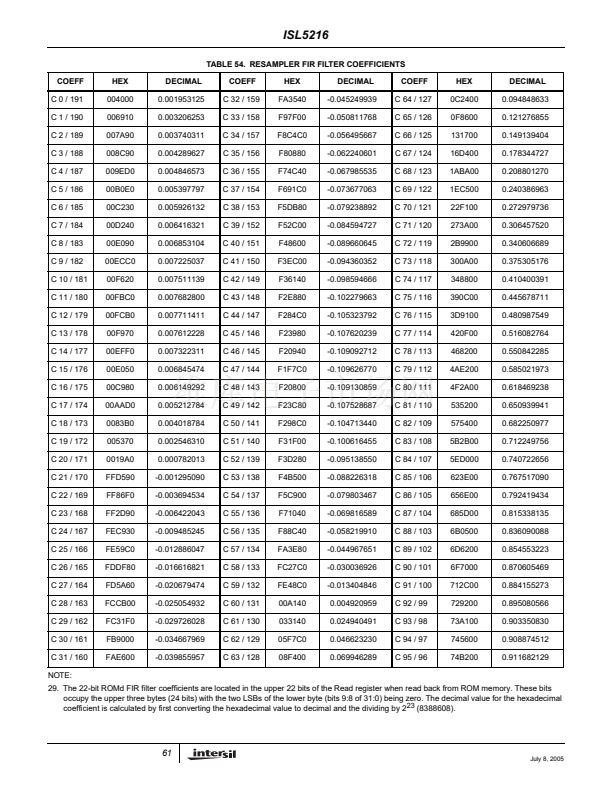
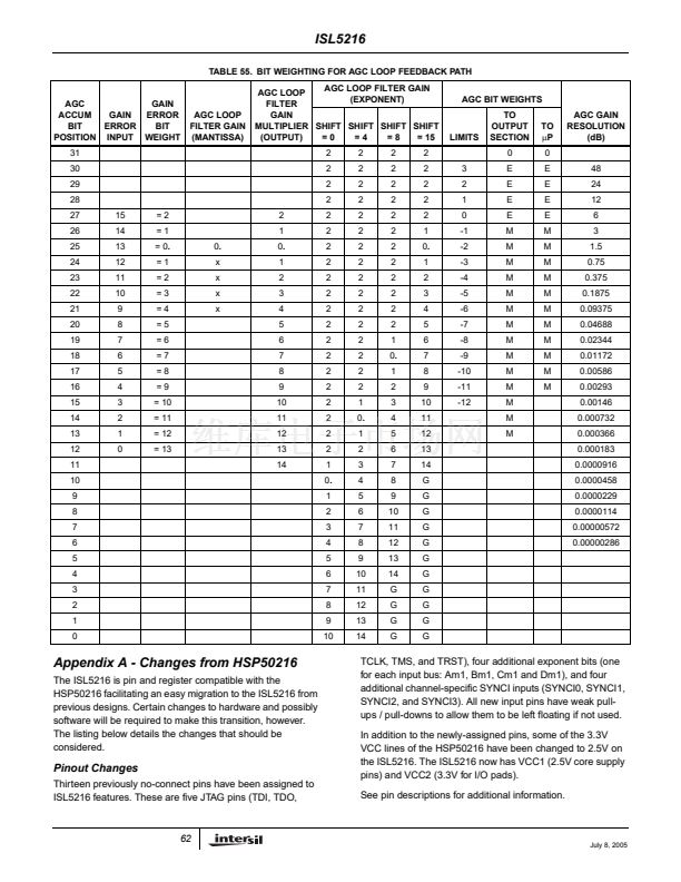
ISL5216
TABLE 7. CIC DECIMATION FACTOR REGISTER (IWA = *002h)
P(15:0)
15:0
Load with the desired CIC decimation factor minus 1.
TABLE 8. CIC DESTINATION FIR AND OUTPUT ENABLE/DISABLE REGISTER (IWA = *003h)
P(15:0)
15:6
5:1
0
FUNCTION
Set to zero.
CIC output destination (FIR # in FIR processor). Usually set to 00001.
CIC output enable. Active high. When low, the data writes from the CIC to the filter compute engine are inhibited.
TABLE 9. CARRIER NCO/CIC CONTROL REGISTER (IWA = *004h)
P(31:0)
31:20
19:14
Reserved, set to zero.
CIC barrel shift control.
000000 is the minimum shift factor and 101111 (47 decimal) is maximum shift factor. 000000 = Shift Factor of 0; 011111 = Shift Factor
of 31; 100000 = Shift Factor of 32; 101111 = Shift Factor of 47. This compensates for the CIC filter gain of R
N
, where N is the number
of enabled CIC stages and R is the CIC decimation factor. The equation used to compute the shift factor is:
Shift Factor = 45 - Ceiling(log
2
(R
N
)). Use a shift of 45 decimal when bypassing the CIC. Note that shifts of 46 and 47 may cause loss
of MSBs.
Examples:
N
R
5
5
13:9
512
8
Shift Factor
0
30
FUNCTION
FUNCTION
CIC stage bypasses. The integrator/comb pairs are numbered 1 thru 5, with 1 being the first integrator and first comb. Bit 13 bypasses
the first integrator/comb pair, bit 12 bypasses the second, etc. The first integrator is the largest. Typically, the stages are enabled
starting with stage 1 for maximum decimation range.
Carrier phase shift. Phase shifts of N*(蟺/4), N = 0 to 7. These bits remain for backward compatibility with the HSP50216. For new
designs, these bits should be set to 0 and the phase offset programmed into IWA *01CH.
Clear feedback (test signal or for mixer bypass).
NCO clear feedback on load.
Update frequency on SYNCI. Redundant. Set to1. See GWA register F802h.
Number of Carrier Offset Frequency (COF) serial input bits. The format is 2鈥檚 complement, early SYNC, MSB first:
00
01
10
11
8
16
24
32
8:6
5
4
3
2:1
0
Enable serial carrier offset frequency (zeros the data already loaded via the COF/COFSYNC pins). To disable the COF shifting see
IWA register *000h.
TABLE 10. CARRIER NCO CENTER FREQUENCY REGISTER (IWA = *005h)
P(31:0)
31:0
Carrier Center Frequency (CCF):
FUNCTION
This is the frequency control for the carrier NCO. The center frequency control is double buffered. The contents of this register are
transferred to the active register on a write to the CCF Strobe location or on a SYNCI (if load on SYNCI is enabled). The carrier center
frequency is: CCF*f
CLK
/(2
32
).
CCF is a twos complement number and has a range of -2
31
to (2
31
-1). f
CLK
is the input sample rate (ENIx assertion rate) for gated
mode and the clock rate for interpolated mode.
The value in the active register can be read at this address (the center frequency control before the serially loaded offset value is
added). To read the value, either write this address to A(1:0) = 11 and then read at A(1:0) = 00 and 01, or read the value at A(1:0) =
00 and 01 after writing to this address and before writing a new address to either A(1:0) = 10 or 11.
36
July 8, 2005


 1
1
 2
2
 3
3
 4
4
 5
5
 6
6
 7
7
 8
8
 9
9
 10
10
 11
11
 12
12
 13
13
 14
14
 15
15
 16
16
 17
17
 18
18
 19
19
 20
20
 21
21
 22
22
 23
23
 24
24
 25
25
 26
26
 27
27
 28
28
 29
29
 30
30
 31
31
 32
32
 33
33
 34
34
 35
35
 36
36
 37
37
 38
38
 39
39
 40
40
 41
41
 42
42
 43
43
 44
44
 45
45
 46
46
 47
47
 48
48
 49
49
 50
50
 51
51
 52
52
 53
53
 54
54
 55
55
 56
56
 57
57
 58
58
 59
59
 60
60
 61
61
 62
62
 63
63
 64
64
 65
65
