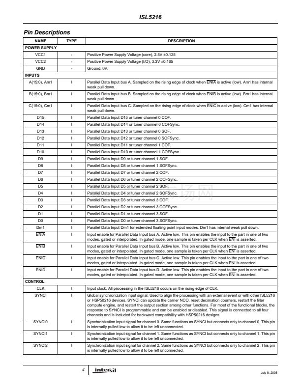
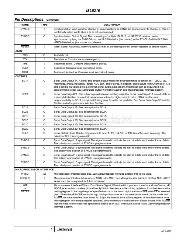
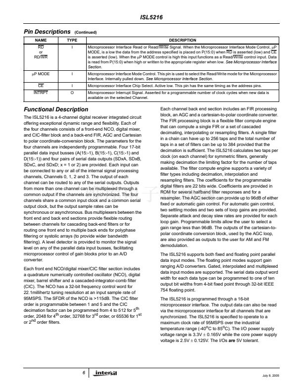
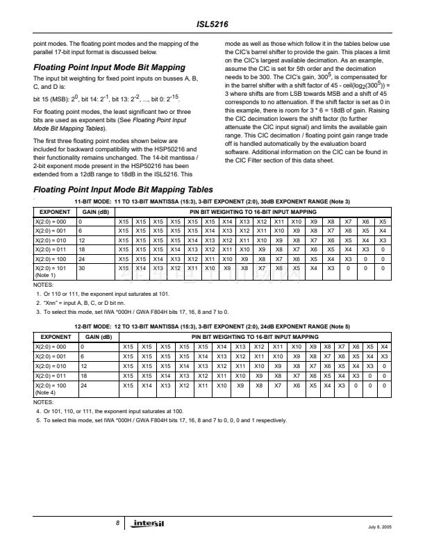
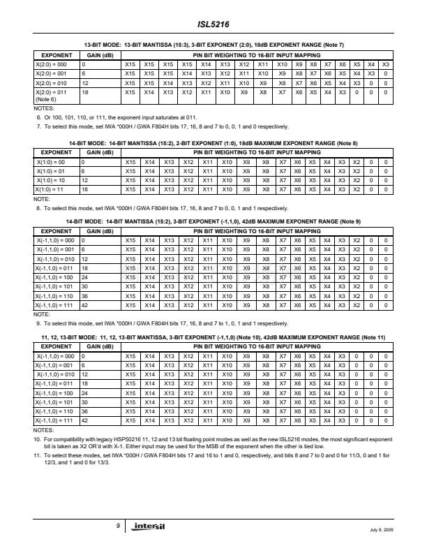
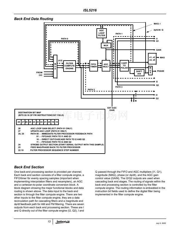
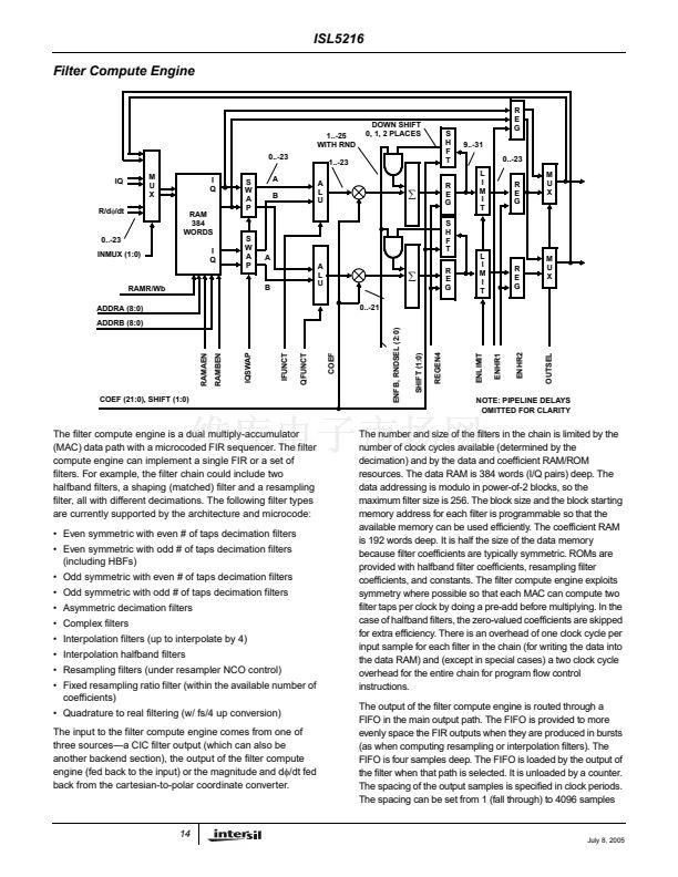
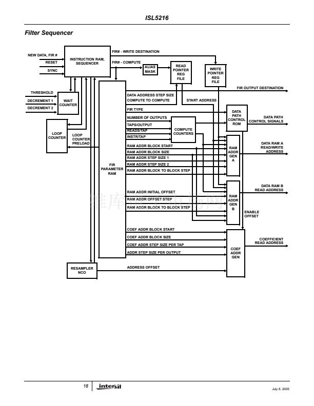
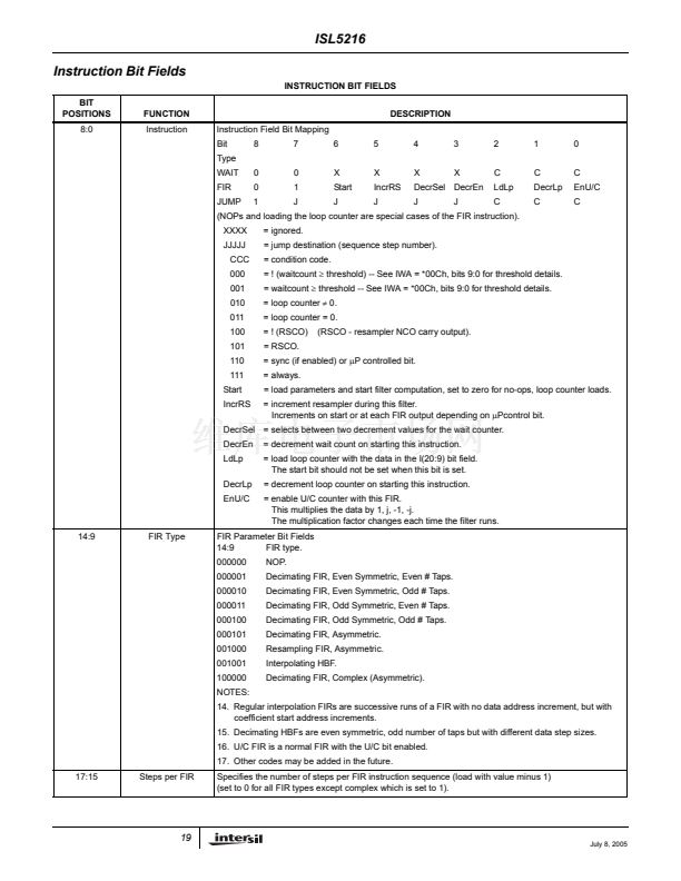
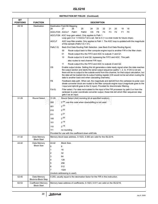
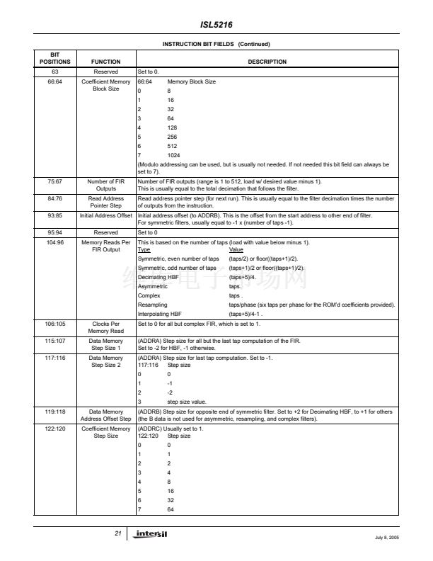
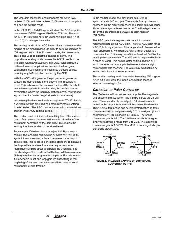
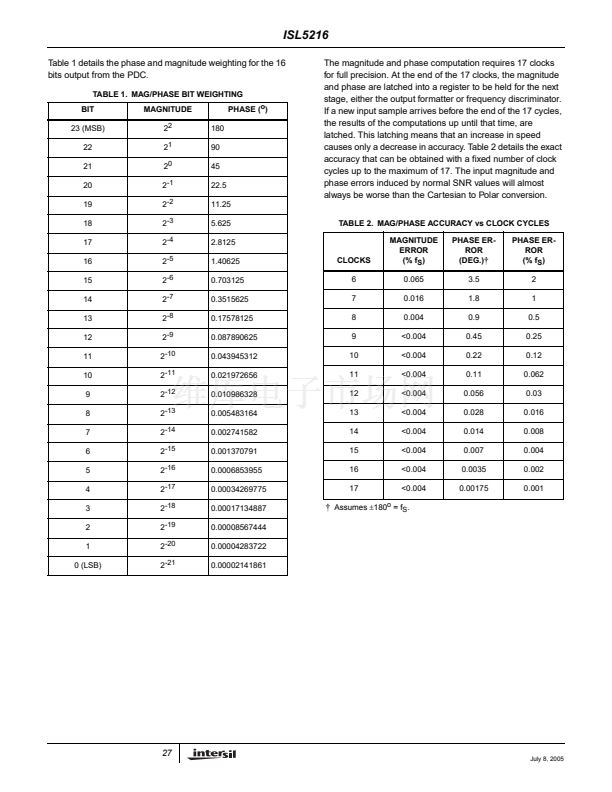
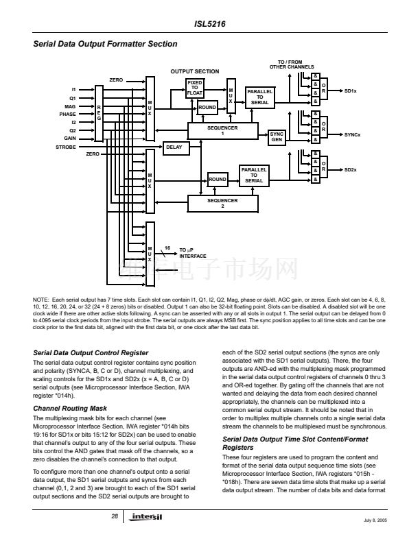
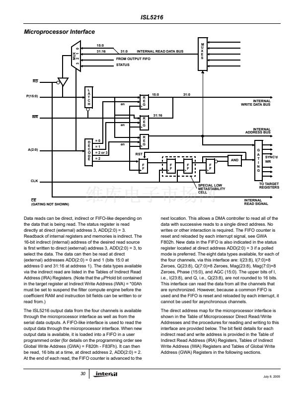
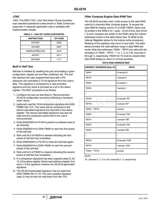
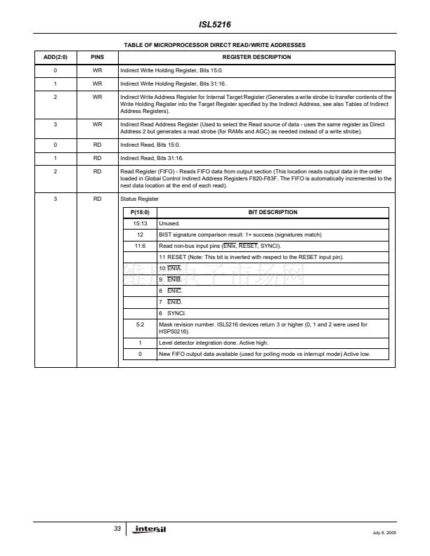
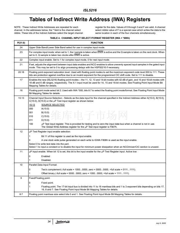
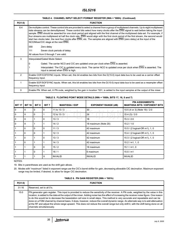
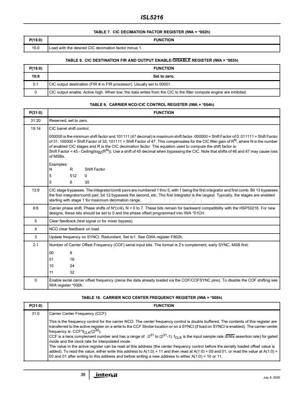
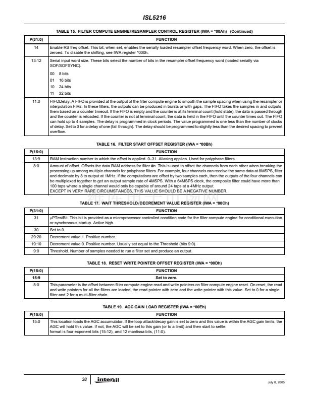
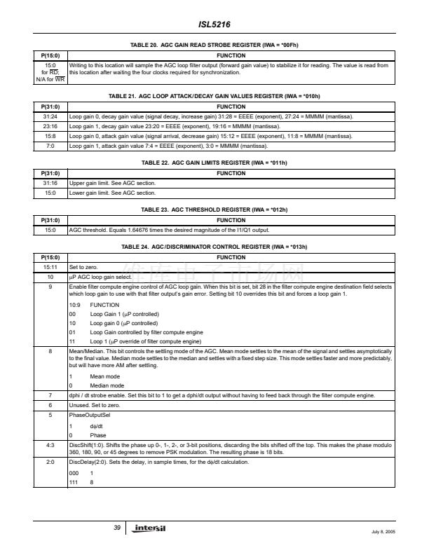
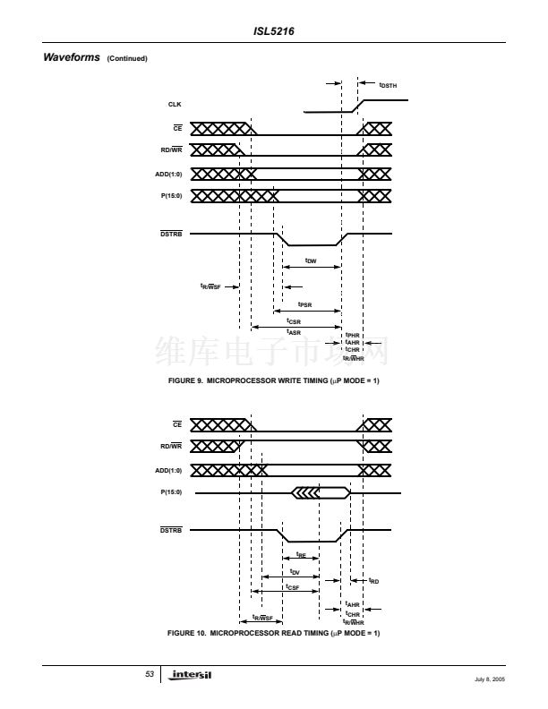
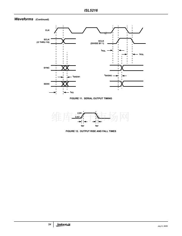
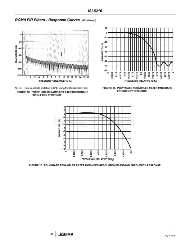
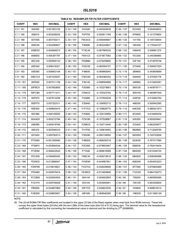
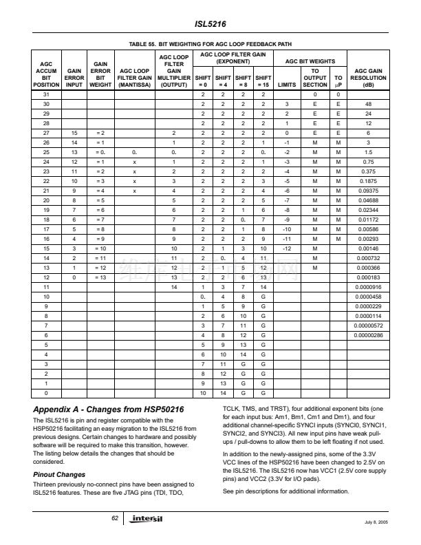
ISL5216
clock and Q * (-SIN) and Q * COS on the second clock cycle.
The first integrator of the CIC is enabled on both clock cycles
to add the two products. The rest of the stages are enabled
only on the first cycle.
In complex input mode, the input level detector uses only I
samples for its magnitude computation.
The CIC decimation counter is programmed for two times the
number of complex input samples. The exponent input must
be the same for I and Q for the floating point modes.
See IWA *000h for details on controlling the complex input
mode.
where S is the sign extension of the 16 bit PN gain register
value (IWA = *001H) times the PN chip value and the 16 X鈥檚
refer to the PN gain register times the PN chip value.
The minimum, non-zero, PN value is 2
-18
of full scale
(-108dBFS) on each axis (-105dBFS total). For an input noise
level of -75dBFS, this allows the SNR to be decreased in
steps of 1/8dB or less. The I and Q PN codes are offset in
time to decorrelate them. The PN code is selected and
enabled in the test control register (F800h). The PN is added
to the signal after the mix with the three sign bits aligned with
the most significant three bits of the signal, so the maximum
level is -12dBFS and the minimum, non-zero level is -
108dBFS. The PN code can be 2
15
-1, 2
23
-1 or 2
15
-1 * 2
23
-1.
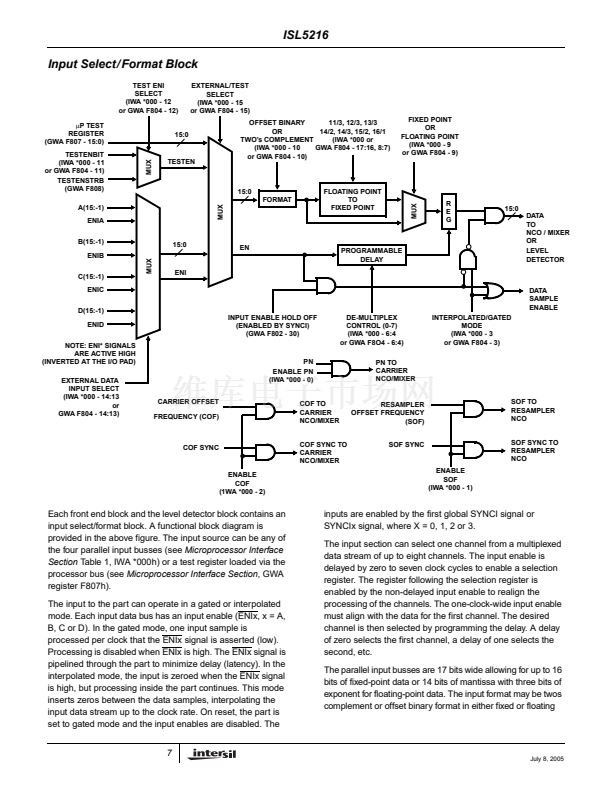
NCO/Mixer
After the input select/format section, the samples are
multiplied by quadrature sine wave samples from the carrier
NCO. The NCO has a 32-bit frequency control, providing
sub-hertz resolution at the maximum clock rate. The
quadrature sinusoids have exceptional purity. The purity of
the NCO should not be the determining factor for the
receiver dynamic range performance. The phase
quantization to the sine/cosine generator is 24 bits and the
amplitude quantization is 19 bits.
The carrier NCO center frequency is loaded via the
碌P
bus.
The center frequency control is double buffered - the input
is loaded into a center frequency holding register via the
碌P
interface. The data is then transferred from the holding
register to the active register by a write to a address IWA
*006h or by a SYNCI signal, if loading via SYNCI is
enabled. To synchronize multiple channels, the carrier NCO
phase accumulator feedback can be zeroed on loading to
restart all of the NCOs at the same phase. A serial offset
frequency input is also available for each channel through
the D(15:0) parallel data input bus (if that bus is not needed
for data input). This is legacy support for HSP50210 type
tracking signals. See IWA=*000 and *004 for carrier offset
frequency parameters.
After the mixers, a PN (pseudo noise) signal can be added to
the data. This feature is provided for test and to digitally
reduce the input sensitivity and adjust the receiver range
(sensitivity). The effect is the same as increasing the noise
figure of the receiver, reducing its sensitivity and overall
dynamic range. For testing, the PN generator provides a
wideband signal which may be used to verify the frequency
response of a filter. The one bit PN data is scaled by a 16-bit
programmable scale factor. The overall range for the PN is 0
to 1/4 full scale (see IWA = *001h). A gain of 0 disables the PN
input. The PN value is formed as:
PN VALUE
2
-3
2
-4 .
S S S
X
X
.
.
.
.
.
.
.
.
.
.
.
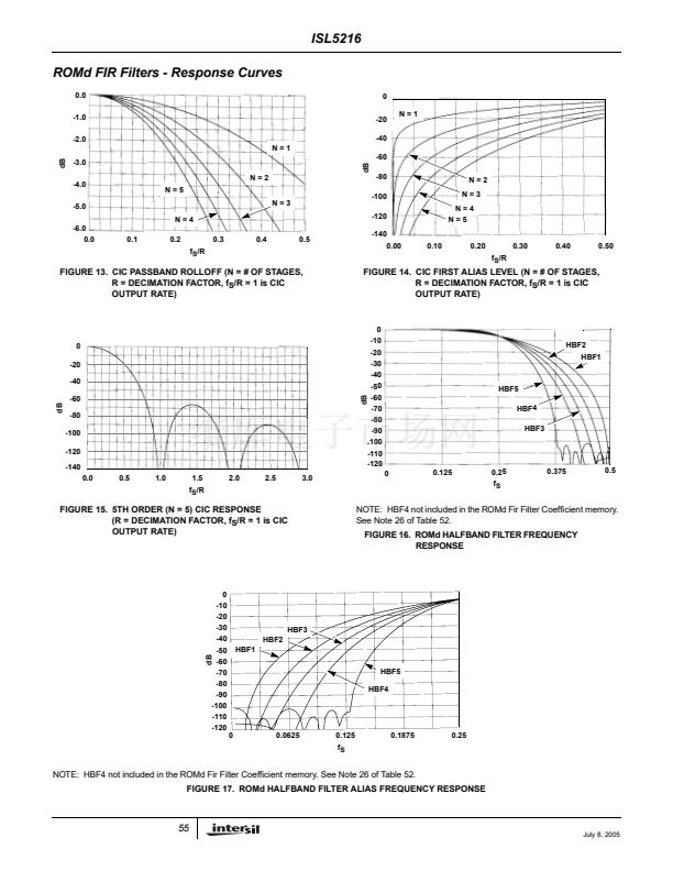
CIC Filter
Next, the signal is filtered by a cascaded integrator/comb
(CIC) filter. A CIC filter is an efficient architecture for
decimation filtering. The power or magnitude squared
frequency response of the CIC filter is given by:
錚?/div>
錚?/div>
2N
錚?/div>
sin
( 蟺Mf )錚?/div>
-
P
(
f
) =
錚?/div>
-----------------------
錚?/div>
錚?/div>
sin
錚?蟺f錚?錚?/div>
----
-
錚?/div>
錚?/div>
R
錚?錚?/div>
where
M = Number of delays (1 for the ISL5216)
N = Number of stages
and R = Decimation factor.
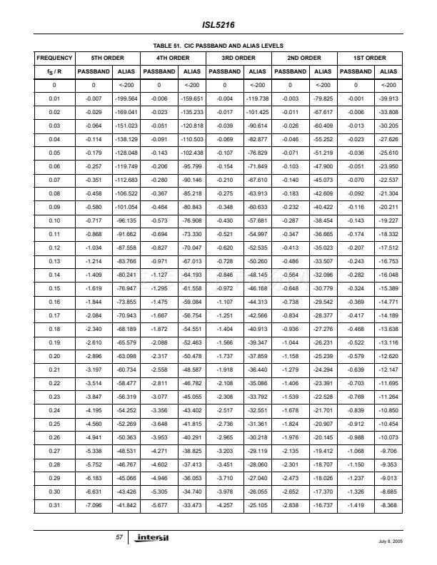
The passband frequency response for first (N=1) though fifth
(N=5) order CIC filters is plotted in Figure 13. The frequency
axis is normalized to f
S
/R, making f
S
/R = 1 the CIC output
sample rate. Figure 15 shows the frequency response for a
5
th
order filter but extends the frequency axis to f
S
/R = 3
(3 times the CIC output sample rate) to show alias rejection
for the out of band signals. Figure 14 uses information from
Figure 15 to provide the amplitude of the first (strongest)
alias as a function of the signal frequency or bandwidth from
DC. For example, with a 5
th
order CIC and f
S
/R = 0.125
(signal frequency is 1/8 the CIC output rate) Figure 14 shows
a first alias level of about -87 dB. Figure 14 is also listed in
table form in Table 51 (CIC Passband and Alias Levels).
The CIC filter order is programmable from 0 to 5. The CIC
may be bypassed by setting the CIC filter order to 0
(IWA = *004h bits 13:9 are all set equal to 1) and the CIC
barrel shift (IWA = *004h bits 19:14) to 45 decimal. The CIC
output rate must, however, be no more than CLK
max
/ 4
where CLK
max
is the maximum clock frequency available on
the device (see electrical specifications section).
The integrator bit widths are 69, 62, 53, 44, and 34 for the
first
t
through fifth stages, respectively, while the comb bit
widths are all 32. The integrators are sized for decimation
factors of up to 512 with five stages, 2048 with four stages,
32768 with three stages, and 65536 with one or two stages.
Higher decimations in the CIC should be avoided as they
will cause integrator overflow. In the ISL5216, the
2
-17
2
-18
X
X
X X X X X X X X X X X X
11
July 8, 2005
ISL5216KIZ 產(chǎn)品屬性
Intersil
+ 85 C
BGA
- 40 C
Tray
ISL5216KIZ相關(guān)型號PDF文件下載
-
型號
版本
描述
廠商
下載
-
英文版
Low-Voltage, Single Supply, Dual SPST, SPDT Analog Switches
-
英文版
Low-Voltage, Single Supply, Dual SPST, SPDT Analog Switches
INTERSIL [...
-
英文版
Low-Voltage, Single Supply, Dual SPST, SPDT Analog Switches
-
英文版
Low-Voltage, Single Supply, Dual SPST, SPDT Analog Switches
INTERSIL [...
-
英文版
Low-Voltage, Single Supply, Dual SPST, SPDT Analog Switches
-
英文版
Low-Voltage, Single Supply, Dual SPST, SPDT Analog Switches
-
英文版
Four-Channel Programmable Digital DownConverter
-
英文版
Quad Programmable Up Converter
-
英文版
Pre-Distortion Linearizer
-
英文版
CommLink Direct Digital Synthesizer
-
英文版
Four-Channel Wideband Programmable DownConverter
-
英文版
3.3V Ringing SLIC Family for Voice Over Broadband (VOB)
-
英文版
Low Power Ringing SLIC for Home Gateways
-
英文版
Dual 8-bit, +3.3V, 260+MSPS, High Speed D/A Converter
-
英文版
Dual 8-bit, +3.3V, 130/210+MSPS, High Speed D/A Converter
-
英文版
3V Dual 8-Bit, 20/40/60MSPS A/D Converter with Internal Volt...
-
英文版
Dual 10-bit, +3.3V, 260+MSPS, High Speed D/A Converter
-
英文版
Dual 10-bit, +3.3V, 130/210+MSPS, High Speed D/A Converter
-
英文版
3V Dual 10-Bit, 20/40/60MSPS A/D Converter with Internal Vol...
-
英文版
10-bit, +3.3V, 260+MSPS, High Speed D/A Converter


 1
1
 2
2
 3
3
 4
4
 5
5
 6
6
 7
7
 8
8
 9
9
 10
10
 11
11
 12
12
 13
13
 14
14
 15
15
 16
16
 17
17
 18
18
 19
19
 20
20
 21
21
 22
22
 23
23
 24
24
 25
25
 26
26
 27
27
 28
28
 29
29
 30
30
 31
31
 32
32
 33
33
 34
34
 35
35
 36
36
 37
37
 38
38
 39
39
 40
40
 41
41
 42
42
 43
43
 44
44
 45
45
 46
46
 47
47
 48
48
 49
49
 50
50
 51
51
 52
52
 53
53
 54
54
 55
55
 56
56
 57
57
 58
58
 59
59
 60
60
 61
61
 62
62
 63
63
 64
64
 65
65
