5. tpd is specified for 50MHz input ref, the window will shrink/grow proportionally from the minimum limit with shorter/longer input reference periods.
The tpd does not include jitter.
APPLICATIONS INFORMATION
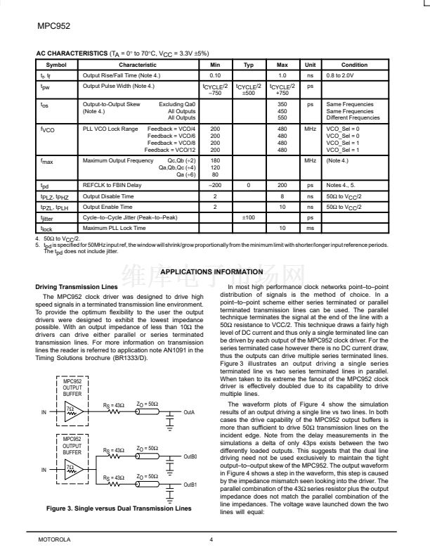
Driving Transmission Lines
The MPC952 clock driver was designed to drive high
speed signals in a terminated transmission line environment.
To provide the optimum flexibility to the user the output
drivers were designed to exhibit the lowest impedance
possible. With an output impedance of less than 10鈩?the
drivers can drive either parallel or series terminated
transmission lines. For more information on transmission
lines the reader is referred to application note AN1091 in the
Timing Solutions brochure (BR1333/D).
In most high performance clock networks point鈥搕o鈥損oint
distribution of signals is the method of choice. In a
point鈥搕o鈥損oint scheme either series terminated or parallel
terminated transmission lines can be used. The parallel
technique terminates the signal at the end of the line with a
50鈩?resistance to VCC/2. This technique draws a fairly high
level of DC current and thus only a single terminated line can
be driven by each output of the MPC952 clock driver. For the
series terminated case however there is no DC current draw,
thus the outputs can drive multiple series terminated lines.
Figure 3 illustrates an output driving a single series
terminated line vs two series terminated lines in parallel.
When taken to its extreme the fanout of the MPC952 clock
driver is effectively doubled due to its capability to drive
multiple lines.
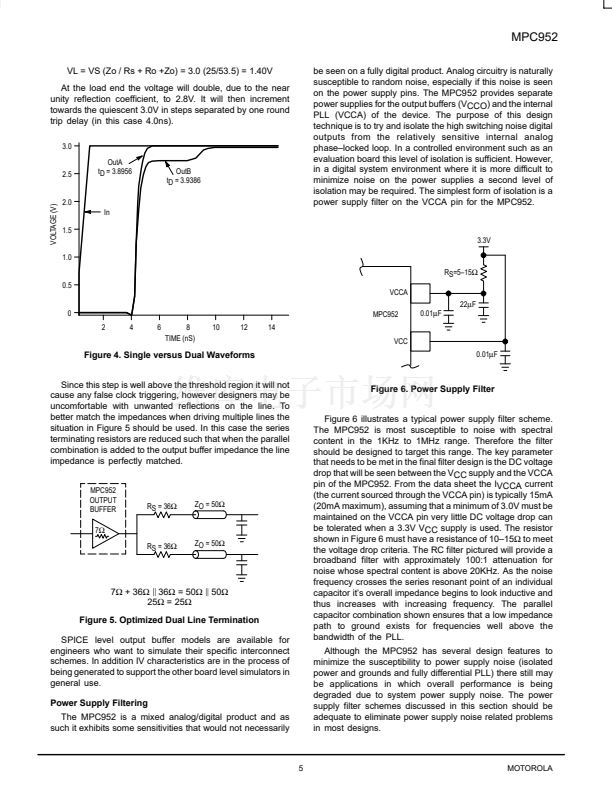
The waveform plots of Figure 4 show the simulation
results of an output driving a single line vs two lines. In both
cases the drive capability of the MPC952 output buffers is
more than sufficient to drive 50鈩?transmission lines on the
incident edge. Note from the delay measurements in the
simulations a delta of only 43ps exists between the two
differently loaded outputs. This suggests that the dual line
driving need not be used exclusively to maintain the tight
output鈥搕o鈥搊utput skew of the MPC952. The output waveform
in Figure 4 shows a step in the waveform, this step is caused
by the impedance mismatch seen looking into the driver. The
parallel combination of the 43鈩?series resistor plus the output
impedance does not match the parallel combination of the
line impedances. The voltage wave launched down the two


 1
1
 2
2
 3
3
 4
4
 5
5
 6
6
 7
7
