MPC952
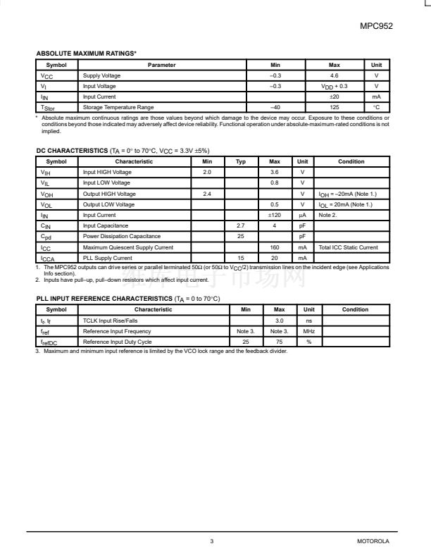
ABSOLUTE MAXIMUM RATINGS*
Symbol
VCC
VI
IIN
TStor
Supply Voltage
Input Voltage
Input Current
Storage Temperature Range
鈥?0
Parameter
Min
鈥?.3
鈥?.3
Max
4.6
VDD + 0.3
鹵20
125
Unit
V
V
mA
擄C
* Absolute maximum continuous ratings are those values beyond which damage to the device may occur. Exposure to these conditions or
conditions beyond those indicated may adversely affect device reliability. Functional operation under absolute-maximum-rated conditions is not
implied.
DC CHARACTERISTICS
(TA = 0擄 to 70擄C, VCC = 3.3V
鹵5%)
Symbol
VIH
VIL
VOH
VOL
IIN
CIN
Cpd
ICC
Characteristic
Input HIGH Voltage
Input LOW Voltage
Output HIGH Voltage
Output LOW Voltage
Input Current
Input Capacitance
Power Dissipation Capacitance
Maximum Quiescent Supply Current
2.7
25
160
2.4
0.5
鹵120
4
Min
2.0
Typ
Max
3.6
0.8
Unit
V
V
V
V
碌A
pF
pF
mA
Total ICC Static Current
IOH = 鈥?0mA (Note 1.)
IOL = 20mA (Note 1.)
Note 2.
Condition
ICCA
PLL Supply Current
15
20
mA
1. The MPC952 outputs can drive series or parallel terminated 50鈩?(or 50鈩?to VCC/2) transmission lines on the incident edge (see Applications
Info section).
2. Inputs have pull鈥搖p, pull鈥揹own resistors which affect input current.
PLL INPUT REFERENCE CHARACTERISTICS
(TA = 0 to 70擄C)
Symbol
tr, tf
fref
Characteristic
TCLK Input Rise/Falls
Reference Input Frequency
Note 3.
Min
Max
3.0
Note 3.
Unit
ns
MHz
%
Condition
frefDC
Reference Input Duty Cycle
25
75
3. Maximum and minimum input reference is limited by the VCO lock range and the feedback divider.
ECLinPS and ECLinPS Lite
DL140 鈥?Rev 3
3
MOTOROLA


 1
1
 2
2
 3
3
 4
4
 5
5
 6
6
 7
7
