-
-

- 手機(jī)版
-

- 芯視頻 APP
-

- 微信公眾號
-

- 維庫官方抖音
-

- 微信頭條號
-
- |
- |
- |
- |

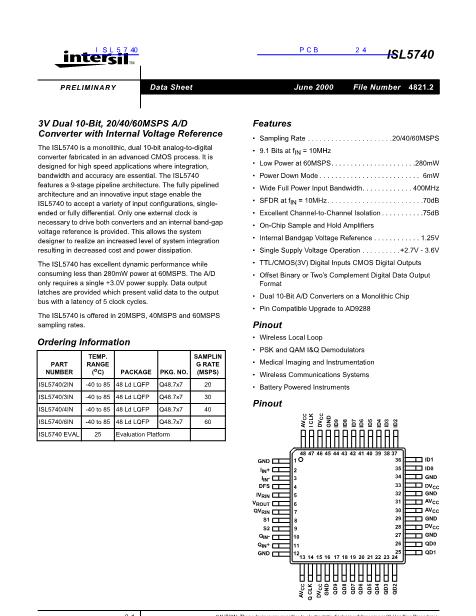
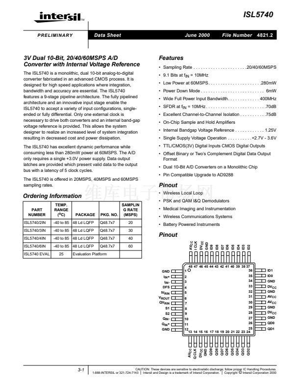
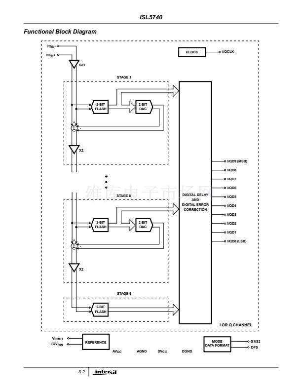
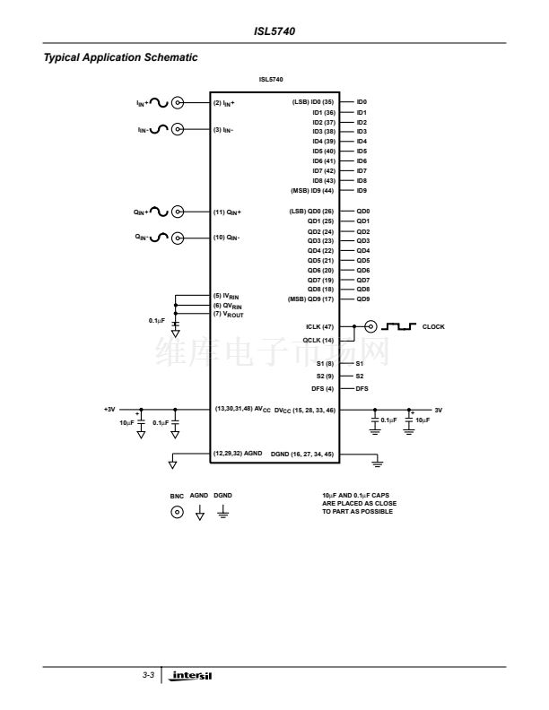
ISL5740
3V Dual 10-Bit, 20/40/60MSPS A/D Converter with Internal Vol...
![]() Intersil
Intersil
掃碼查看芯片數(shù)據(jù)手冊
上傳產(chǎn)品規(guī)格書


聯(lián)系人:
聯(lián)系方式:

 1
1
 2
2
 3
3
 4
4
 5
5
 6
6
 7
7
 8
8
 9
9
 10
10
 11
11
 12
12
