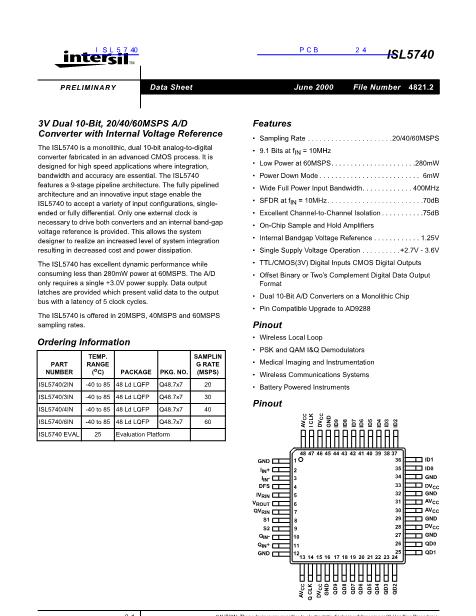
ISL5740
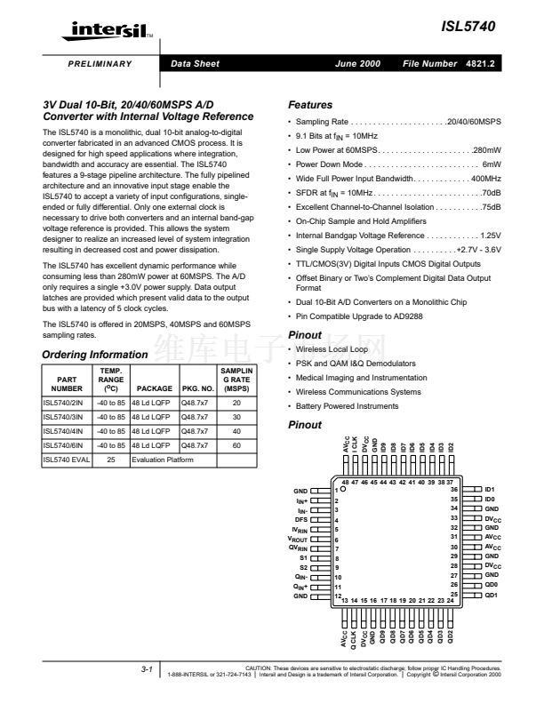
Pin Descriptions
PIN NO.
1
2
3
4
NAME
A
GND
I
IN+
I
IN-
DFS
DESCRIPTION
Analog Ground
I-Channel Positive Analog Input
I-Channel Negative Analog Input
Data Format Select (Low for Offset
Binary and High for Twos Complement
Output Format)
I-Channel Voltage Reference Input
+1.25V Reference Voltage Output
(Decouple with 0.1碌F Capacitor)
Q-Channel Voltage Reference Input
Mode Select Pin 1 (See Table)
Mode Select Pin 2 (See Table)
Q-Channel Negative Analog Input
Q-Channel Positive Analog Input
Analog Ground
Analog Supply
Q-Channel Clock Input
Digital Supply
Digital Ground
Q-Channel, Data Bit 9 Output (MSB)
Q-Channel, Data Bit 8 Output
Q-Channel, Data Bit 7 Output
Q-Channel, Data Bit 6 Output
Q-Channel, Data Bit 5 Output
Q-Channel, Data Bit 4 Output
Q-Channel, Data Bit 3 Output
Pin Descriptions
PIN NO.
24
25
26
27
28
29
30
31
32
33
34
35
36
37
38
39
40
41
42
43
44
45
46
47
48
NAME
QD2
QD1
QD0
D
GND
DV
CC
A
GND
AV
CC
AV
CC
A
GND
DV
CC
D
GND
ID0
ID1
ID2
ID3
ID4
ID5
ID6
ID7
ID8
ID9
D
GND
DV
CC
ICLK
AV
CC
(Continued)
DESCRIPTION
Q-Channel, Data Bit 2 Output
Q-Channel, Data Bit 1 Output
Q-Channel, Data Bit 0 Output (LSB)
Digital Ground
Digital Supply
Analog Ground
Analog Supply
Analog Supply
Analog Ground
Digital Supply
Digital Ground
I-Channel, Data Bit 0 Output (LSB)
I-Channel, Data Bit 1 Output
I-Channel, Data Bit 2 Output
I-Channel, Data Bit 3 Output
I-Channel, Data Bit 4 Output
I-Channel, Data Bit 5 Output
I-Channel, Data Bit 6 Output
I-Channel, Data Bit 7 Output
I-Channel, Data Bit 8 Output
I-Channel, Data Bit 9 Output (MSB)
Digital Ground
Digital Supply
I-Channel Clock Input
Analog Supply
5
6
7
8
9
10
11
12
13
14
15
16
17
18
19
20
21
22
23
IV
RIN
V
ROUT
QV
RIN
S1
S2
Q
IN-
Q
IN+
A
GND
AV
CC
QCLK
DV
CC
D
GND
QD9
QD8
QD7
QD6
QD5
QD4
QD3
3-4


 1
1
 2
2
 3
3
 4
4
 5
5
 6
6
 7
7
 8
8
 9
9
 10
10
 11
11
 12
12
