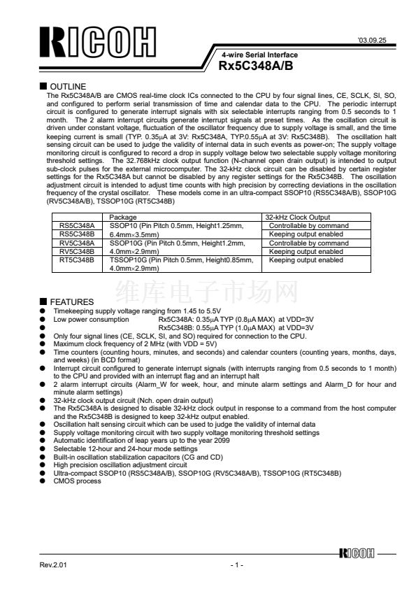
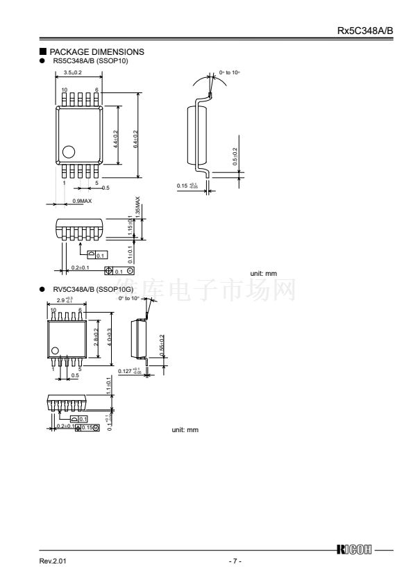
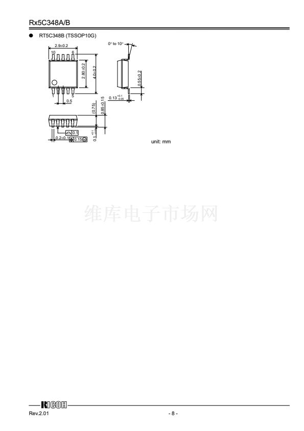
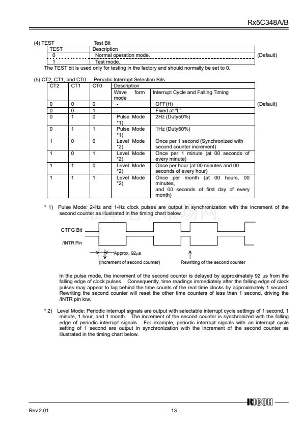
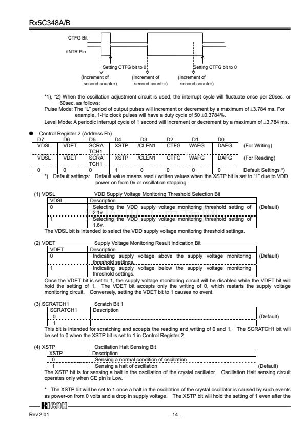
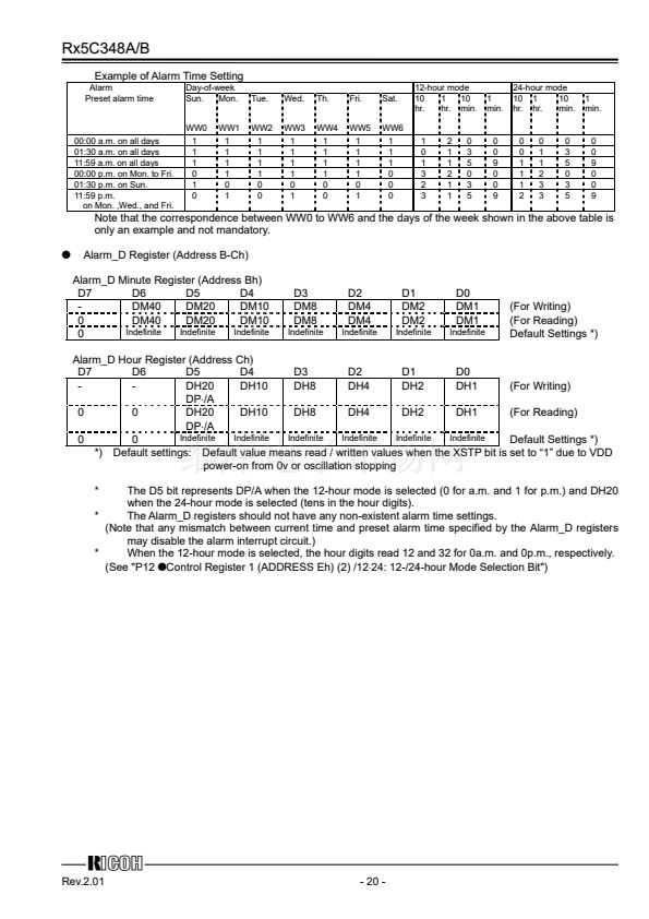
Rx5C348A/B
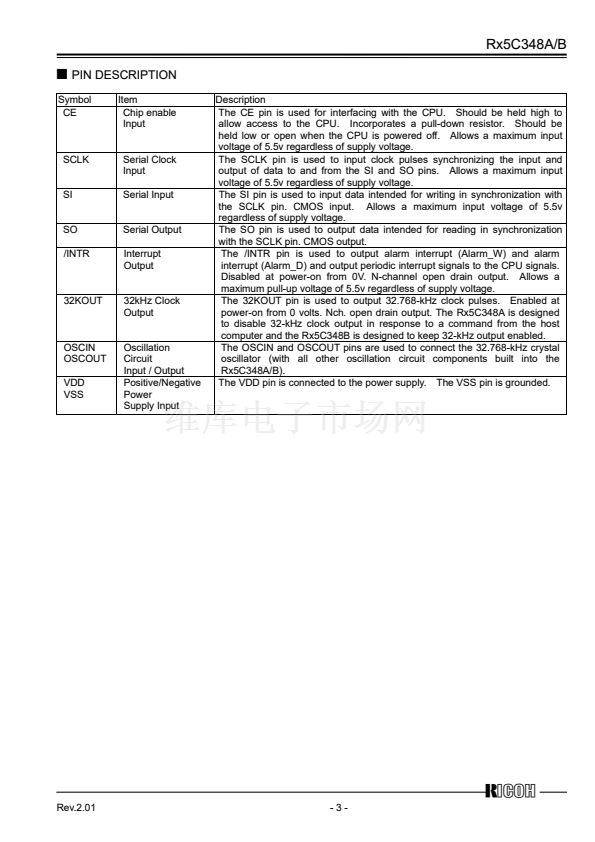
Interfacing with the CPU
DATA TRANSFER FORMATS
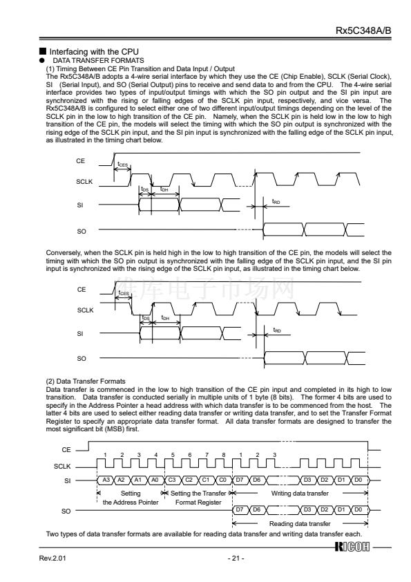
(1) Timing Between CE Pin Transition and Data Input / Output
The Rx5C348A/B adopts a 4-wire serial interface by which they use the CE (Chip Enable), SCLK (Serial Clock),
SI (Serial Input), and SO (Serial Output) pins to receive and send data to and from the CPU. The 4-wire serial
interface provides two types of input/output timings with which the SO pin output and the SI pin input are
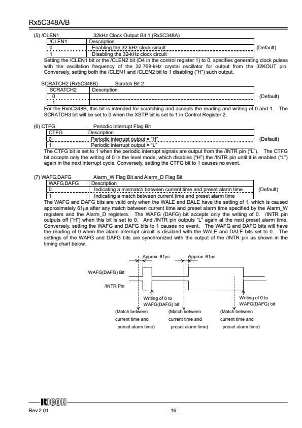
synchronized with the rising or falling edges of the SCLK pin input, respectively, and vice versa. The
Rx5C348A/B is configured to select either one of two different input/output timings depending on the level of the
SCLK pin in the low to high transition of the CE pin. Namely, when the SCLK pin is held low in the low to high
transition of the CE pin, the models will select the timing with which the SO pin output is synchronized with the
rising edge of the SCLK pin input, and the SI pin input is synchronized with the falling edge of the SCLK pin input,
as illustrated in the timing chart below.
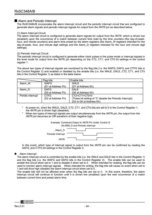
CE
SCLK
t
DS
SI
t
DH
t
RD
t
CES
SO
Conversely, when the SCLK pin is held high in the low to high transition of the CE pin, the models will select the
timing with which the SO pin output is synchronized with the falling edge of the SCLK pin input, and the SI pin
input is synchronized with the rising edge of the SCLK pin input, as illustrated in the timing chart below.
CE
SCLK
t
DS
SI
t
DH
t
RD
t
CES
SO
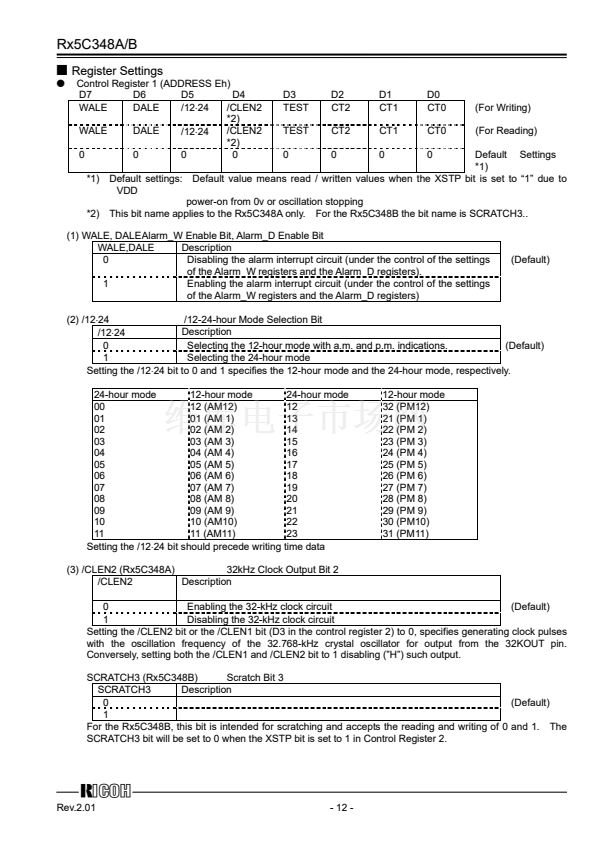
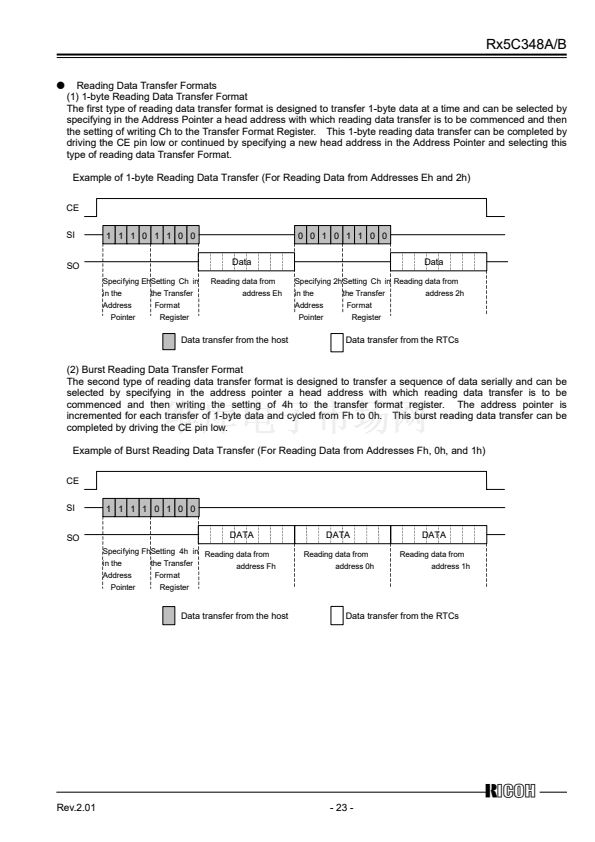
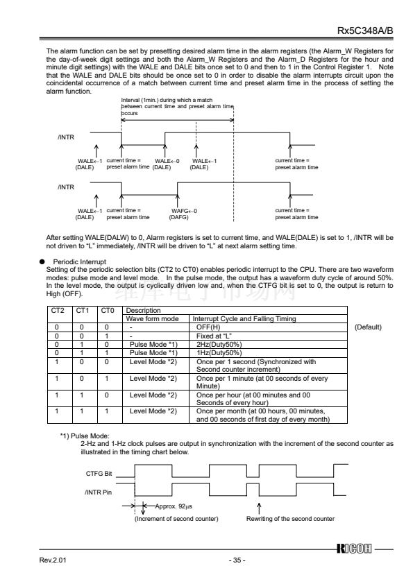
(2) Data Transfer Formats
Data transfer is commenced in the low to high transition of the CE pin input and completed in its high to low
transition. Data transfer is conducted serially in multiple units of 1 byte (8 bits). The former 4 bits are used to
specify in the Address Pointer a head address with which data transfer is to be commenced from the host. The
latter 4 bits are used to select either reading data transfer or writing data transfer, and to set the Transfer Format
Register to specify an appropriate data transfer format. All data transfer formats are designed to transfer the
most significant bit (MSB) first.
CE
SCLK
SI
A3
1
2
3
4
5
6
7
8
1
2
3
A2
A1
A0
C3
C2
C1
C0
D7
D6
D3
D2
D1
D0
Setting
the Address Pointer
Setting the Transfer
Format Register
D7
D6
Writing data transfer
D3
D2
D1
D0
SO
Reading data transfer
Two types of data transfer formats are available for reading data transfer and writing data transfer each.
12345
Rev.2.01
- 21 -


 1
1
 2
2
 3
3
 4
4
 5
5
 6
6
 7
7
 8
8
 9
9
 10
10
 11
11
 12
12
 13
13
 14
14
 15
15
 16
16
 17
17
 18
18
 19
19
 20
20
 21
21
 22
22
 23
23
 24
24
 25
25
 26
26
 27
27
 28
28
 29
29
 30
30
 31
31
 32
32
 33
33
 34
34
 35
35
 36
36
 37
37
 38
38
 39
39
 40
40
 41
41
 42
42
 43
43
 44
44
 45
45
