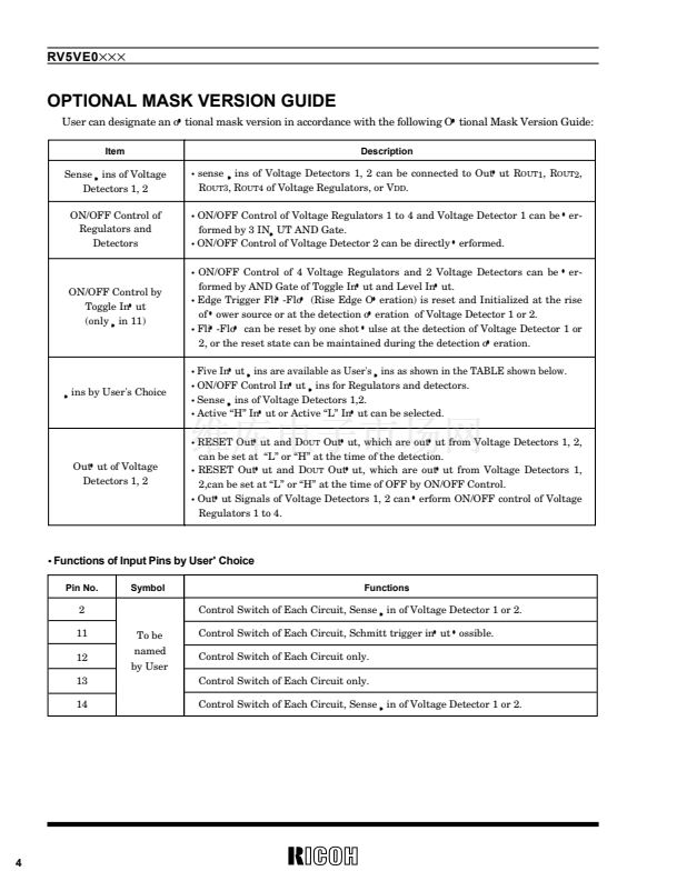
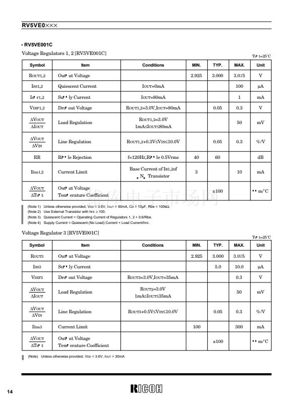
鈥?/div>
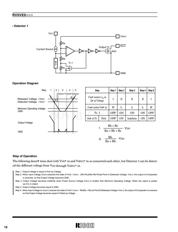
Vref
Rb
Tr.1
Rc
GND
C
D
Output Capacitor
Tr.2
Rb
RESET
Operation Diagram
Step
1
2
3
4
B
A
5
Step
Step 1
Step 2
Step 3
Step 4
Step 5
Detector Threshold Hysteresis
Released Voltage +V
DET
Detected Voltage 鈥揤
DET
Minimum Operating Voltage
GND
Comparato (+) Pin
Input Voltage
Comparator Output
Tr. 1
Output Tr.
Nch
I
.
I
H
OFF
OFF
II
L
ON
ON
II
L
ON
Indefinite
II
L
ON
ON
I
H
OFF
OFF
Output Voltage
Delay Time
Rb + Rc
Ra + Rb + Rc
路 V
DD
GND
II.
Rb
Ra + Rb
路 V
DD
Step of Operation
The following descriptions deal with V
DD
pin and V
SEN
2
pin as connected each other, but Detector 2 can be detect-
ed the different voltage from V
DD
through V
SEN
2
pin.
Step 1. Output Voltage is equal to Pull-up Voltage.
Step 2. When Input Voltage (V
SEN
2
) reaches the state of Vref
鈮?/div>
V
SEN
2
路 (Rb+Rc)/(Ra+Rb+Rc)at Point A (Detected Voltage 鈥?V
DET
), the output of Compara-
tor is reversed, so that Output Voltage becomes GND. Discharging is performed from C
D
pin connected to External Capacitor. No delay time is
generated.
Step 3. Output Voltage becomes indefinite when Power Source Voltage (V
DD
) is smaller than Minimum Operating Voltage. When the output is pulled-
up,V
DD
is output.
Step 4. Output Voltage becomes equal to GND.
Step 5. When Input Voltage (V
SEN
2
) reaches the state of Vref鈮
SEN
2
路 Rb/(Ra + Rb) at Point B (Released Voltage +V
DET
), the output of Comparator is reversed, and
the External Capacitor is charged through C
D
pin,so that Output Voltage becomes equal to Pulled-up Voltage after a delay timeT
D
(= 0.69
脳
10
6
脳
C
D
).
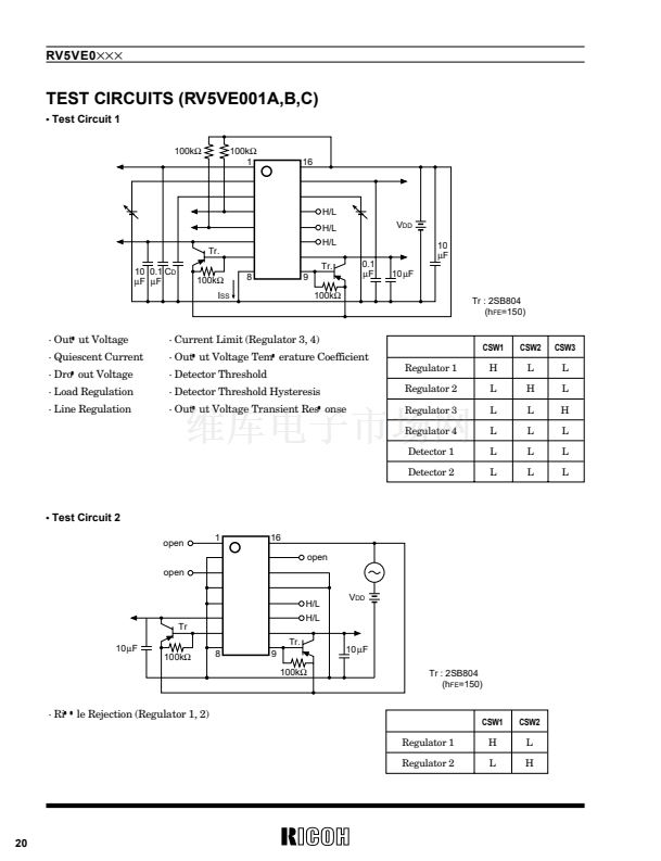
19


 1
1
 2
2
 3
3
 4
4
 5
5
 6
6
 7
7
 8
8
 9
9
 10
10
 11
11
 12
12
 13
13
 14
14
 15
15
 16
16
 17
17
 18
18
 19
19
 20
20
 21
21
 22
22
 23
23
 24
24
 25
25
 26
26
 27
27
 28
28
 29
29
 30
30
 31
31
 32
32
 33
33
 34
34
 35
35
 36
36
 37
37
 38
38
 39
39
 40
40
 41
41
 42
42
 43
43
 44
44
 45
45
 46
46
 47
47
 48
48
 49
49
