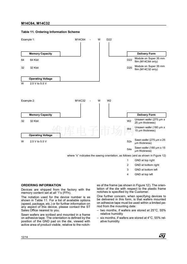
M14C64, M14C32
SIGNAL DESCRIPTION
Serial Clock (SCL)
The SCL input pin is used to synchronize all data
in and out of the memory. A pull up resistor can be
connected from the SCL line to V
CC
. (Figure 4 in-
dicates how the value of the pull-up resistor can be
calculated).
Serial Data (SDA)
The SDA pin is bi-directional, and is used to trans-
fer data in or out of the memory. It is an open drain
output that may be wire-OR鈥檈d with other open
drain or open collector signals on the bus. A pull
up resistor must be connected from the SDA bus
to V
CC
. (Figure 4 indicates how the value of the
pull-up resistor can be calculated).
Write Control (WC)
The hardware Write Control contact (WC) is useful
for protecting the entire contents of the memory
from inadvertent erase/write. The Write Control
signal is used to enable (WC=V
IL
) or disable
(WC=V
IH
) write instructions to the entire memory
area. When unconnected, the WC input is internal-
ly read as V
IL
and write operations are allowed.
When WC=1, Device Select and Address bytes
are acknowledged, Data bytes are not acknowl-
edged.
Please see the Application Note
AN404
for a more
detailed description of the Write Control feature.
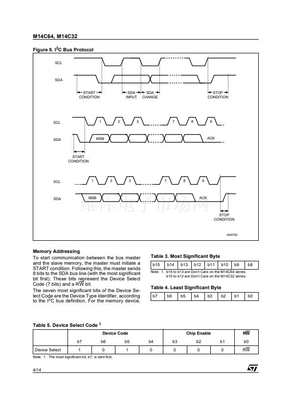
DEVICE OPERATION
The memory device supports the XI
2
C (Extended
I
2
C) protocol, as summarized in Figure 5. Any de-
vice that sends data on to the bus is defined to be
a transmitter, and any device that reads the data
to be a receiver. The device that controls the data
transfer is known as the master, and the other as
the slave. A data transfer can only be initiated by
the master, which will also provide the serial clock
for synchronization. The memory device is always
a slave device in all communication.
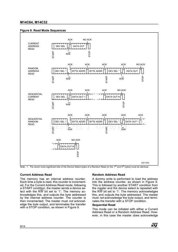
Start Condition
START is identified by a high to low transition of
the SDA line while the clock, SCL, is stable in the
high state. A START condition must precede any
data transfer command. The memory device con-
tinuously monitors (except during a programming
cycle) the SDA and SCL lines for a START condi-
tion, and will not respond unless one is given.
Stop Condition
STOP is identified by a low to high transition of the
SDA line while the clock SCL is stable in the high
state. A STOP condition terminates communica-
tion between the memory device and the bus mas-
ter. A STOP condition at the end of a Read
command, after (and only after) a NoACK, forces
the memory device into its standby state. A STOP
condition at the end of a Write command triggers
the internal EEPROM write cycle.
Acknowledge Bit (ACK)
An acknowledge signal is used to indicate a suc-
cessful data transfer. The bus transmitter, either
master or slave, will release the SDA bus after
sending 8 bits of data. During the 9
th
clock pulse
period the receiver pulls the SDA bus low to ac-
knowledge the receipt of the 8 data bits.
Data Input
During data input, the memory device samples the
SDA bus signal on the rising edge of the clock,
SCL. For correct device operation, the SDA signal
must be stable during the clock low-to-high transi-
tion, and the data must change
only
when the SCL
line is low.
Figure 4. Maximum R
L
Value versus Bus Capacitance (C
BUS
) for an I
2
C Bus
VCC
20
Maximum RP value (k鈩?
16
RL
12
8
4
0
10
100
CBUS (pF)
AI01665
RL
SDA
MASTER
fc = 100kHz
fc = 400kHz
SCL
CBUS
CBUS
1000
3/14


 1
1
 2
2
 3
3
 4
4
 5
5
 6
6
 7
7
 8
8
 9
9
 10
10
 11
11
 12
12
 13
13
 14
14
