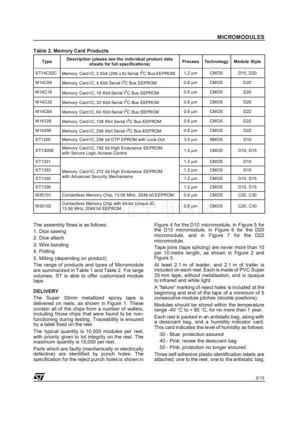
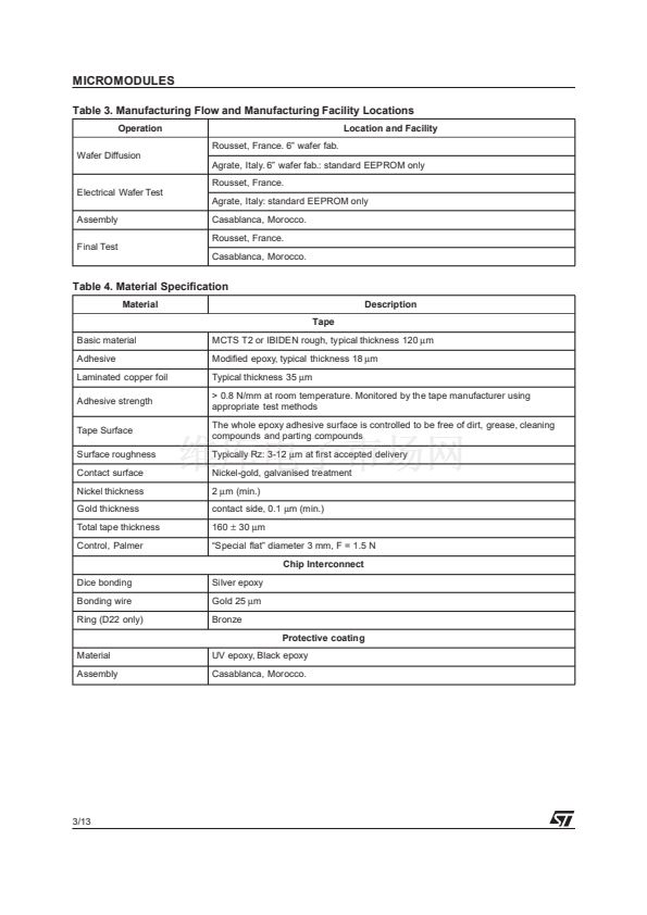
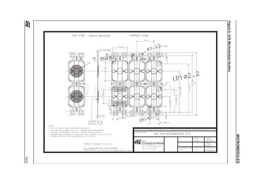
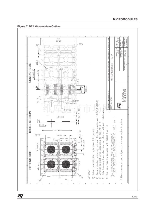
MICROMODULES
Table 3. Manufacturing Flow and Manufacturing Facility Locations
Operation
Rousset, France. 6鈥?wafer fab.
Wafer Diffusion
Agrate, Italy. 6鈥?wafer fab.: standard EEPROM only
Rousset, France.
Electrical Wafer Test
Agrate, Italy: standard EEPROM only
Assembly
Final Test
Casablanca, Morocco.
Casablanca, Morocco.
Rousset, France.
Location and Facility
Table 4. Material Specification
Material
Tape
Basic material
Adhesive
Laminated copper foil
Adhesive strength
Tape Surface
Surface roughness
Contact surface
Nickel thickness
Gold thickness
Total tape thickness
Control, Palmer
MCTS T2 or IBIDEN rough, typical thickness 120
碌m
Modified epoxy, typical thickness 18
碌m
Typical thickness 35
碌m
> 0.8 N/mm at room temperature. Monitored by the tape manufacturer using
appropriate test methods
The whole epoxy adhesive surface is controlled to be free of dirt, grease, cleaning
compounds and parting compounds
Typically Rz: 3-12
碌m
at first accepted delivery
Nickel-gold, galvanised treatment
2
碌m
(min.)
contact side, 0.1
碌m
(min.)
160
鹵
30
碌m
鈥淪pecial flat鈥?diameter 3 mm, F = 1.5 N
Chip Interconnect
Dice bonding
Bonding wire
Ring (D22 only)
Silver epoxy
Gold 25
碌m
Bronze
Protective coating
Material
Assembly
UV epoxy, Black epoxy
Casablanca, Morocco.
Description
3/13


 1
1
 2
2
 3
3
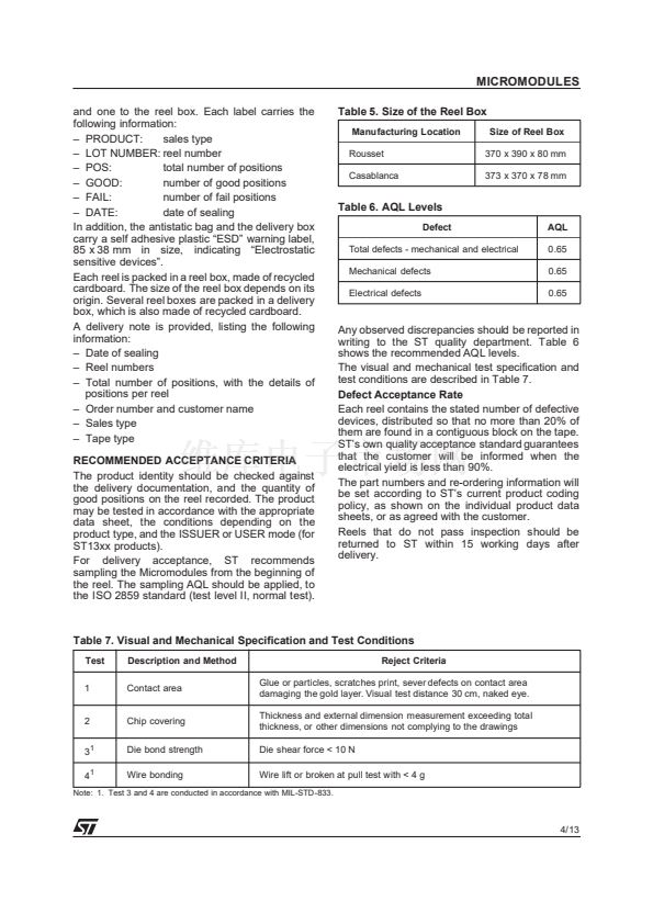 4
4
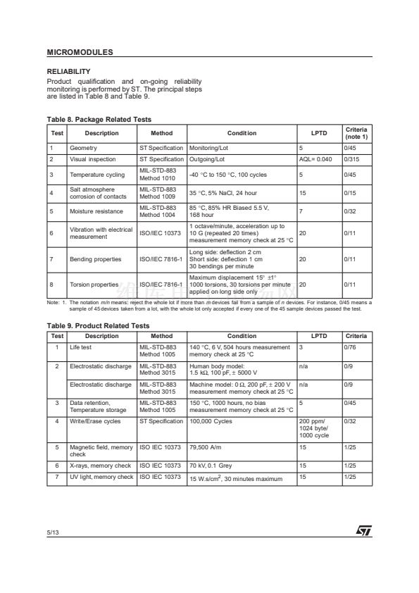 5
5
 6
6
 7
7
 8
8
 9
9
 10
10
 11
11
 12
12
 13
13
