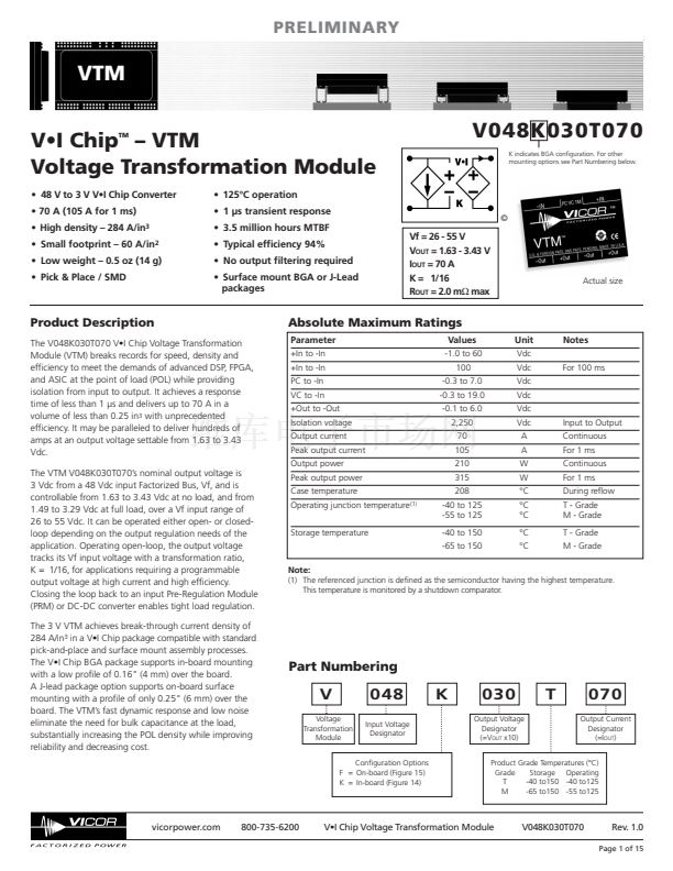
PRELIMINARY
Electrical Specifications
Input Specs
(Conditions are at 48 Vin, full load, and 25擄C ambient unless otherwise specified)
Parameter
Input voltage range
Input dV/dt
Input overvoltage turn-on
Input overvoltage turn-off
Input current
Input reflected ripple current
No load power dissipation
Internal input capacitance
Internal input inductance
182
3.3
4
20
4.56
55
60
4.8
V鈥 Chip Voltage Transformation Module
Min
26
Typ
48
Max
55
1
Unit
Vdc
V/碌s
Vdc
Vdc
Adc
mA p-p
W
碌F
nH
Note
Operable down to zero V with VC voltage applied
Using test circuit in Figure 16; See Figure 1
Output Specs
(Conditions are at 48 Vin, full load, and 25擄C ambient unless otherwise specified)
Parameter
Output voltage
Rated DC current
Peak repetitive current
DC current limit
Current share accuracy
Efficiency
Half load
Full load
Internal output inductance
Internal output capacitance
Output overvoltage setpoint
Output ripple voltage
No external bypass
10 碌F bypass capacitor
Effective switching frequency
Line regulation
K
Load regulation
R
OUT
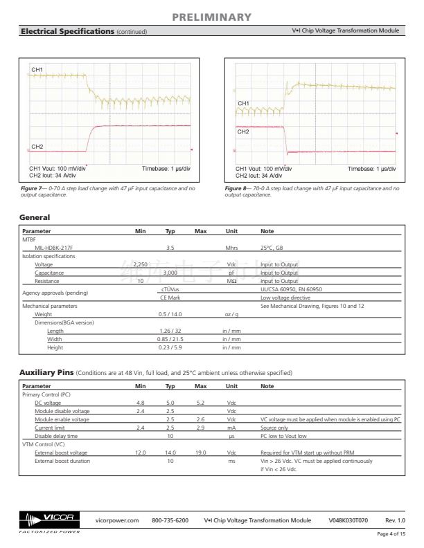
Transient response
Voltage overshoot
Response time
Recovery time
66
200
1
mV
ns
碌s
70 A load step with 100 碌F C
IN
; See Figures 7 and 8
See Figures 7 and 8
See Figures 7 and 8
1.8
2.0
m鈩?/div>
See Figure 19
0.0619
1/16
0.0631
V
OUT
= K鈥
IN
at no load
2.5
80
8.6
2.6
2.8
100
mV
mV
MHz
See Figures 2 and 5
See Figure 6
Fixed, 1.3 MHz per phase
3.4
94.0
93.5
94.5
94.1
1.1
254
%
%
nH
碌F
Vdc
Effective value
See Figure 3
See Figure 3
71.4
87.1
5
Min
1.63
1.49
0
Typ
Max
3.43
3.29
70
105
94.5
10
Unit
Vdc
Vdc
Adc
A
Adc
%
Note
No load
Full load
Max pulse width 1ms, max duty cycle 10%,
baseline power 50%
Module will shut down when current limit is reached
or exceeded
See Parallel Operation on Page 10
vicorpower.com
800-735-6200
V鈥 Chip Voltage Transformation Module
V048K030T070
Rev. 1.0
Page 2 of 15


 1
1
 2
2
 3
3
 4
4
 5
5
 6
6
 7
7
 8
8
 9
9
 10
10
 11
11
 12
12
 13
13
 14
14
 15
15
