voltage range should not be exceeded. The V鈥 Chip BCM鈥檚
outside of the normal input range. The BCM turns ON within an
turn-on" and "Input over-voltage turn-off" levels, as specified.
positive input located on the load side of the input fuse.
used on-board across the +IN and 鈥揑N pins. The type of
such as an electrolytic capacitor. If ceramic capacitance is
鈩?/div>
series resistance.
Anomalies in the response of the source will appear at the
output of the IBC multiplied by its K factor. The DC resistance
of the source should be kept as low as possible to minimize
voltage deviations. This is especially important if the IBC is
operated near low or high line as the over/under voltage
detection circuitry of the BCM(s) could be activated.
PC 鈥?Primary Control Pin
The Primary Control pin is a multifunction node that provides
the following functions:
Enable/Disable
Standard "P" configuration 鈥?If the PC pin is left floating, the
BCM output is enabled. Once this port is pulled lower than 2.4 Vdc
with respect to 鈥揑N, the output is disabled. This action can be
realized by employing a relay, opto-coupler or open collector
transistor. This port should not be toggled at a rate higher than 1 Hz.
Optional "M" configuration 鈥?This is the reverse function as
above: when the PC pin is left floating , the BCM output is
disabled.
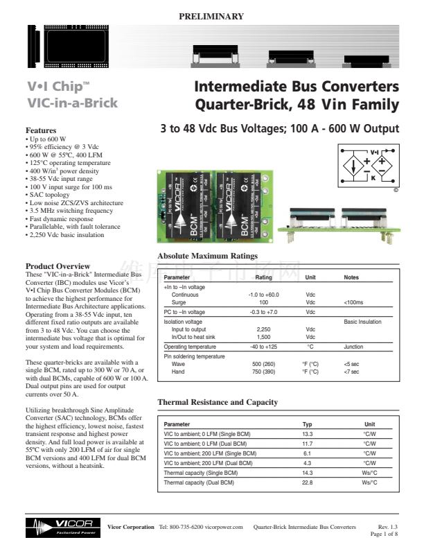
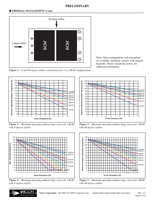
THERMAL MANAGEMENT
Figures 2 to 5 provide the IBC鈥檚 maximum ambient operating
temperature vs. BCM power dissipation for a variety of airflows.
In order to determine the maximum ambient environment for a
given application, the following procedure should be used:
1. Determine the maximum load powered by the IBC.
2. Determine the power dissipated at this load by the
on-board BCM(s).
a) If using a 1 BCM configuration, this dissipation is
found in Fig. 6 on the appropriate BCM data sheet
corresponding to the output voltage of the IBC.
b) If using a 2 BCM configuration, divide the maximum
load by 2. The power dissipated by each BCM is found in
4. Using the chart corresponding to the appropriate airflow
angle, find the curve corresponding to the airflow
velocity and read the maximum ambient operating
temperature of the IBC (y-axis) based on the total BCM
power dissipation (x-axis).
For additional information on V鈥 Chip thermal design, please
read the "Thermal Management" section of the BCM data sheet.
Quarter-Brick Intermediate Bus Converters
Rev. 1.3
Page 5 of 8
Primary Auxiliary Supply 鈥?The PC pin can source up to
2.4 mA at 5.0 Vdc. (P version only)
Alarm 鈥?The BCM contains watchdog circuitry that monitors
output overload, input over voltage or under voltage, and
internal junction temperatures. In response to an abnormal
condition in any of the monitored parameters, the PC pin
will toggle. (P version only)
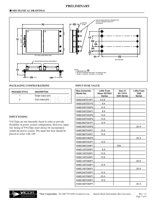
+OUT / 鈥?OUT 鈥?DC Voltage Output Pins
The 0.062" diameter + and 鈥?output pins are rated for a
maximum current of 50 A. Two sets of pins are provided for all
units with a current rating over 50 A. These pins must be
connected in parallel with minimal interconnect resistance.
Within the specified operating range, the average output voltage
is defined by the Level 1 DC behavioral model of the on board
BCM(s) as defined in the appropriate BCM data sheet.
Output impedance
The very low output impedance of the IBC, as shown in the
Product Matrix table, reduces or eliminates the need for limited
life aluminum electrolytic or tantalum capacitors at the input of
the non-isolated point-of-load converters.
Load capacitance
Total load capacitance at the output of the IBC should not
exceed the specified maximum as shown in the Product Matrix
table. Owing to the wide bandwidth and low output impedance
of the BCM, low frequency bypass capacitance and significant
energy storage may be more densely and efficiently provided by
adding capacitance at the input of the IBC.
Bi-directional operation
The BCM power train and control architecture allow bi-
directional power transfer, including reverse power processing
from the BCM output to its input. Reverse power transfer is
enabled if the BCM input is within its operating range and the
BCM is otherwise enabled. The BCM鈥檚 ability to process power
in reverse significantly improves the IBC transient response to
an output load dump.
Fig. 6 on the appropriate BCM data sheet corresponding
to the output voltage of the IBC. This number should
then be multiplied by 2 to reflect the total dissipation.
3. Determine the airflow orientation from Fig.1.
Vicor Corporation
Tel: 800-735-6200 vicorpower.com
Factorized Power


 1
1
 2
2
 3
3
 4
4
 5
5
 6
6
 7
7
 8
8
