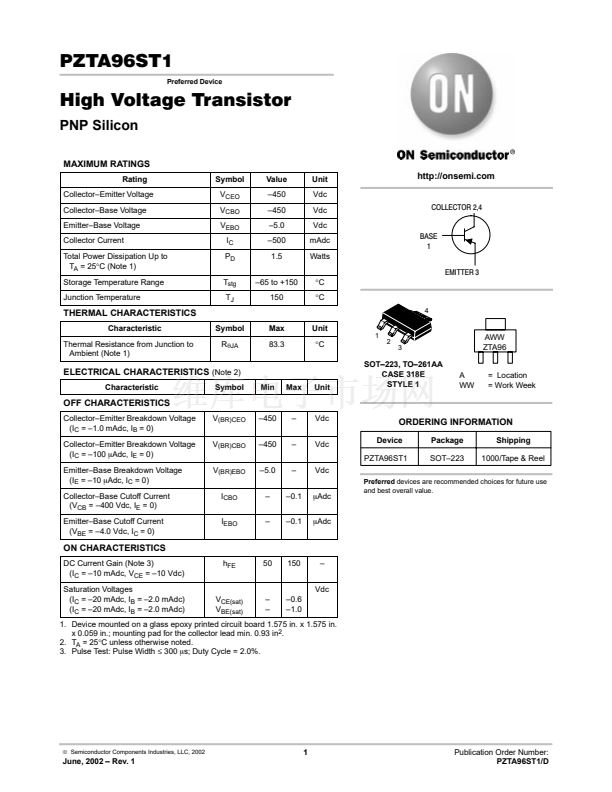
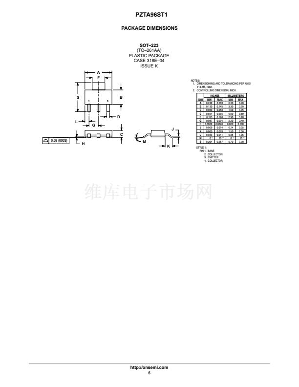
PZTA96ST1
INFORMATION FOR USING THE SOT鈥?23 SURFACE MOUNT PACKAGE
MINIMUM RECOMMENDED FOOTPRINT FOR SURFACE MOUNTED APPLICATIONS
Surface mount board layout is a critical portion of the total
design. The footprint for the semiconductor packages must
be the correct size to insure proper solder connection
0.15
3.8
0.079
2.0
0.248
6.3
interface between the board and the package. With the
correct pad geometry, the packages will self align when
subjected to a solder reflow process.
SOT鈥?23
0.091
2.3
0.091
2.3
0.079
2.0
0.059
1.5
0.059
1.5
0.059
1.5
mm
inches
SOT鈥?23 POWER DISSIPATION
The power dissipation of the SOT鈥?23 is a function of
the pad size. This can vary from the minimum pad size for
soldering to the pad size given for maximum power dissipa-
tion. Power dissipation for a surface mount device is deter-
mined by T
J(max)
, the maximum rated junction temperature
of the die, Rq
JA
, the thermal resistance from the device
junction to ambient; and the operating temperature, T
A
. Us-
ing the values provided on the data sheet for the SOT鈥?23
package, P
D
can be calculated as follows.
P
D
=
T
J(max)
鈥?T
A
R
qJA
doubled with this method, area is taken up on the printed
circuit board which can defeat the purpose of using
surface mount technology. A graph of R
qJA
versus collec-
tor pad area is shown in Figure 1.
160
R JA , Thermal Resistance, Junction
to Ambient ( C/W)
Board Material = 0.0625鈥?/div>
G 10/FR 4, 2 oz Copper
0.8 Watts
T
A
= 25擄C
140
擄
120
1.25 Watts*
1.5 Watts
The values for the equation are found in the maximum
ratings table on the data sheet. Substituting these values into
the equation for an ambient temperature T
A
of 25擄C, one
can calculate the power dissipation of the device which in
this case is 1.5 watts.
P
D
=
150擄C 鈥?25擄C
83.3擄C/W
= 1.50 watts
100
*Mounted on the DPAK footprint
0.2
0.4
0.6
A, Area (square inches)
0.8
1.0
胃
80
0.0
The 83.3擄C/W for the SOT-223 package assumes the
use of the recommended footprint on a glass epoxy
printed circuit board to achieve a power dissipation of 1.5
watts. There are other alternatives to achieving higher
power dissipation from the SOT-223 package. One is to
increase the area of the collector pad. By increasing the
area of the collector pad, the power dissipation can be
increased. Although the power dissipation can almost be
Figure 1. Thermal Resistance versus Collector
Pad Area for the SOT-223 Package (Typical)
Another alternative would be to use a ceramic substrate
or an aluminum core board such as Thermal Clad鈩? Using
a board material such as Thermal Clad, an aluminum core
board, the power dissipation can be doubled using the same
footprint.
http://onsemi.com
2


 1
1
 2
2
 3
3
 4
4
 5
5
 6
6
 7
7
 8
8
