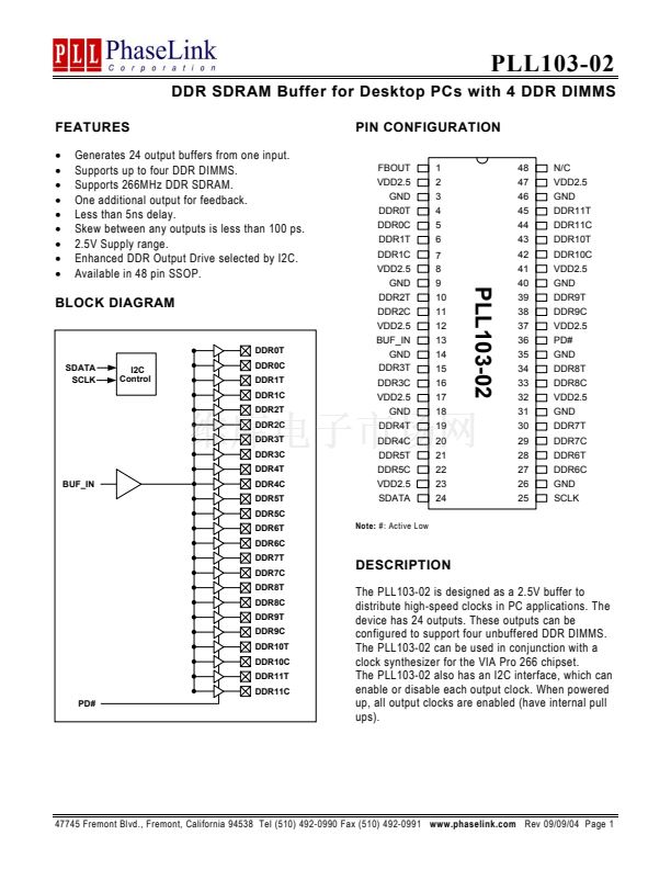
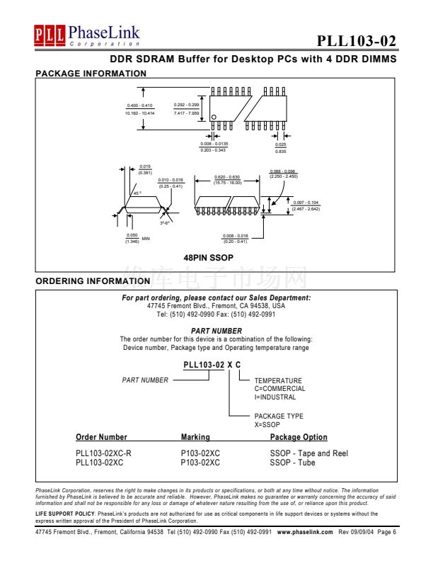
PLL103-02
DDR SDRAM Buffer for Desktop PCs with 4 DDR DIMMS
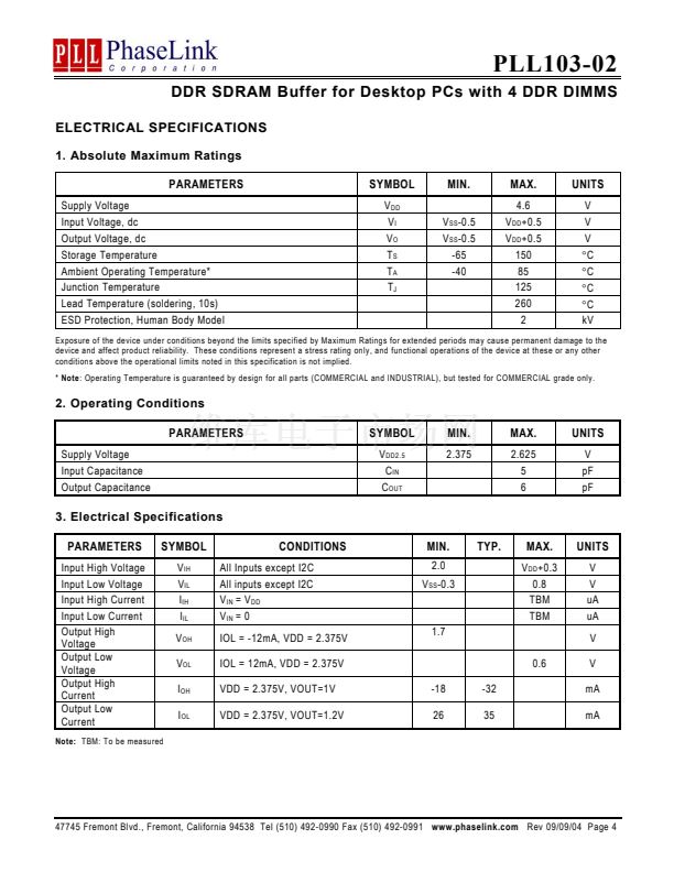
ELECTRICAL SPECIFICATIONS
1. Absolute Maximum Ratings
PARAMETERS
Supply Voltage
Input Voltage, dc
Output Voltage, dc
Storage Temperature
Ambient Operating Temperature*
Junction Temperature
Lead Temperature (soldering, 10s)
ESD Protection, Human Body Model
SYMBOL
V
DD
V
I
V
O
T
S
T
A
T
J
MIN.
V
SS
-0.5
V
SS
-0.5
-65
-40
MAX.
4.6
V
DD
+0.5
V
DD
+0.5
150
85
125
260
2
UNITS
V
V
V
擄C
擄C
擄C
擄C
kV
Exposure of the device under conditions beyond the limits specified by Maximum Ratings for extended periods may cause permanent damage to the
device and affect product reliability. These conditions represent a stress rating only, and functional operations of the device at these or any other
conditions above the operational limits noted in this specification is not implied.
*
Note:
Operating Temperature is guaranteed by design for all parts (COMMERCIAL and INDUSTRIAL), but tested for COMMERCIAL grade only.
2. Operating Conditions
PARAMETERS
Supply Voltage
Input Capacitance
Output Capacitance
SYMBOL
V
DD2.5
C
IN
C
OUT
MIN.
2.375
MAX.
2.625
5
6
UNITS
V
pF
pF
3. Electrical Specifications
PARAMETERS
Input High Voltage
Input Low Voltage
Input High Current
Input Low Current
Output High
Voltage
Output Low
Voltage
Output High
Current
Output Low
Current
Note:
TBM: To be measured
SYMBOL
V
IH
V
IL
I
IH
I
IL
V
OH
V
OL
I
OH
I
OL
CONDITIONS
All Inputs except I2C
All inputs except I2C
V
IN
= V
DD
V
IN
= 0
IOL = -12mA, VDD = 2.375V
IOL = 12mA, VDD = 2.375V
VDD = 2.375V, VOUT=1V
VDD = 2.375V, VOUT=1.2V
MIN.
2.0
V
SS
-0.3
TYP.
MAX.
V
DD
+0.3
0.8
TBM
TBM
UNITS
V
V
uA
uA
V
1.7
0.6
-18
26
-32
35
V
mA
mA
47745 Fremont Blvd., Fremont, California 94538 Tel (510) 492-0990 Fax (510) 492-0991
www.phaselink.com
Rev 09/09/04 Page 4


 1
1
 2
2
 3
3
 4
4
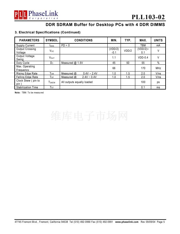 5
5
 6
6
