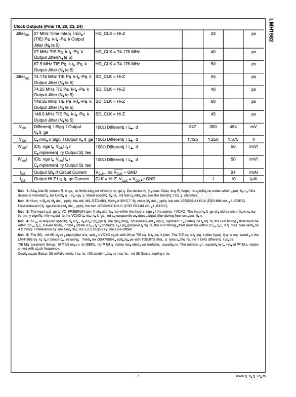
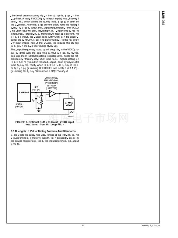
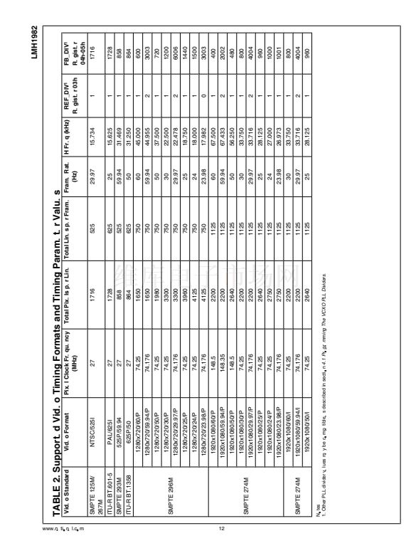
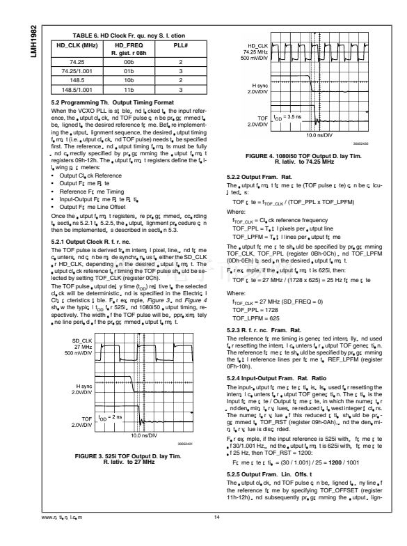
LMH1982
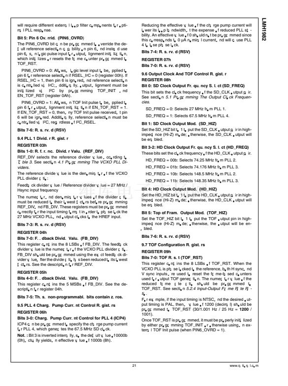
REGISTER 0Ah
Bits 4-0: TOF Reset (TOF_RST)
This register contains the 5 MSBs of TOF_RST. See the de-
scription for register 09h.
Bit 5: Output Alignment Initialization (TOF_INIT)
After enabling output alignment mode (EN_TOF_RST = 1),
the TOF_INIT bit should be programmed to initially align the
outputs to the desired input reference frame. The initialization
is triggered by programming a positive bit transition (0 to 1) to
TOF_INIT, which will reset the frame counters programmed
to TOF_RST. See section
5.3 Programming The Output
Alignment Sequence.
Bit 6: TOF Pulse Output Polarity (POL_TOF)
This bit should be programmed to the desired TOF pulse po-
larity at the TOF output.
POL_TOF = 0: Negative polarity or active low signal.
POL_TOF = 1: Positive polarity or active high signal.
Bit 7: Output Alignment Mode (EN_TOF_RST)
This bit must be set (EN_TOF_RST = 1) to enable output
alignment mode prior to initialization per section
5.3 Program-
ming The Output Alignment Sequence.
It is recommended to
clear this bit (EN_TOF_RST = 0) immediately after the output
alignment sequence has been programmed to prevent ex-
cessive output jitter, as described in section
2.3 Output Dis-
turbance While Alignment Mode Enabled.
REGISTER 0Bh
Bits 7-0: Total Pixels per Line for the Output Format
(TOF_PPL)
This register contains the 8 LSBs of TOF_PPL. TOF_PPL
should be programmed with total pixels per line for the desired
output format. TOF_PPL is used in specifying the output
frame rate. This should be specified prior to programming the
output alignment sequence. See section
5.2.2 Output Frame
Rate.
REGISTER 0Ch
Bits 4-0: MSBs of Total Pixels per Line for the Output
Format (TOF_PPL)
This register contains the 5 MSBs of TOF_PPL. See the de-
scription for register 0Bh.
Bit 5: Reference Clock Select for Output Top of Frame
(TOF_CLK)
This bit should be programmed to select the output clock ref-
erence according to the desired output format. The selected
clock frequency is used in specifying the output frame rate.
See sections
5.2.1 Output Clock Reference
and
5.2.2 Output
Frame Rate.
TOF_CLK = 0: Selects the SD_CLK output as the output
clock reference.
TOF_CLK = 1: Selects the HD_CLK output as the output
clock reference.
Bit 7-6: These non-programmable bits contain zeros.
REGISTER 0Dh
Bits 7-0: LSBs of Total Lines per Frame for the Output
Format (TOF_LPFM)
This register contains the 8 LSBs of TOF_LPFM. TOF_LPFM
should be programmed with the total lines per frame for the
desired output format. TOF_LPFM is used in specifying the
output frame rate. This should be specified prior to program-
ming the output alignment sequence. See section
5.2.2 Out-
put Frame Rate.
REGISTER 0Eh
Bits 3-0: MSBs of Total Lines per Frame for the Output
Format (TOF_LPFM)
This register contains the 4 MSBs of TOF_LPFM. See the
description for register 0Dh.
Bit 7-5: These non-programmable bits contain zeros.
REGISTER 0Fh
Bits 7-0: LSBs of Total Lines per Frame for the Input Ref-
erence Format (REF_LPFM)
This register contains the 8 LSBs of REF_LPFM. REF_LPFM
should be programmed with the total lines per frame for the
input reference format. REF_LPFM is used in specifying the
reference frame rate. This should be specified prior to pro-
gramming the output alignment sequence (section
5.2.3 Ref-
erence Frame Rate).
REGISTER 10h
Bits 3-0: MSBs of Total Lines per Frame for the Input Ref-
erence Format (REF_LPFM)
This register contains the 4 MSBs of REF_LPFM. See the
description for register 0Fh.
Bit 7-4: These non-programmable bits contain zeros.
REGISTER 11h
Bits 7-0: LSBs of Output Frame Offset (TOF_OFFSET)
This register contains the 8 LSBs of TOF_OFFSET.
TOF_OFFSET should be programmed with the desired line
offset to delay or advance the output timing relative to the
reference frame. This should be specified prior to program-
ming the output alignment sequence. See section
5.2.5 Out-
put Frame Line Offset.
REGISTER 12h
Bits 3-0: MSBs of Line Offset for the Output Top of Frame
(TOF_OFFSET)
This register contains the 4 MSBs of TOF_OFFSET. See the
description for register 11h.
Bit 7-4: These bits contain zeros (non-programmable)
9.8 PLL 1 Charge Pump Current Control Register
REGISTER 13h
Bits 4-0: Charge Pump Current Control for PLL 1 (ICP1)
ICP1 can be programmed to specify the charge pump current
for PLL 1. ICP1 is one of the loop gain parameters can be
programmed to optimize the VCXO PLL loop response.
For example, ICP1 can be adjusted in proportion to a change
in FB_DIV to maintain a constant loop gain and a thus con-
sistent loop response across different input formats for the
same loop filter circuit. Also, when phase lock has been
achieved, lowering ICP1 can reduce the PLL1 charge pump
current to lower the loop bandwidth for additional input jitter
rejection; this can be helpful to minimize low-frequency input
jitter from propagating to the output clocks.
Note:
ICP1 values of 0 to 2 correspond to PLL 1 charge pump
currents of less than about 60 碌A(chǔ). These low currents may
cause reduced PLL performance (e.g. loss of lock, clock wan-
der) due to loop filter charge leakage and other secondary
factors. Therefore, it is not recommended to use ICP1 less
than 3.
ICP1 = 0: 0 碌A(chǔ) (not recommended)
www.national.com
22


 1
1
 2
2
 3
3
 4
4
 5
5
 6
6
 7
7
 8
8
 9
9
 10
10
 11
11
 12
12
 13
13
 14
14
 15
15
 16
16
 17
17
 18
18
 19
19
 20
20
 21
21
 22
22
 23
23
 24
24
 25
25
 26
26
 27
27
 28
28
