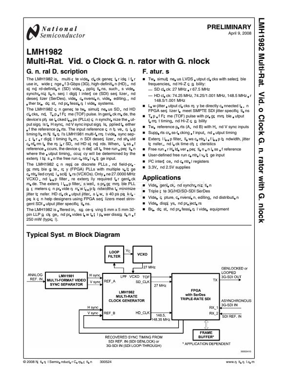
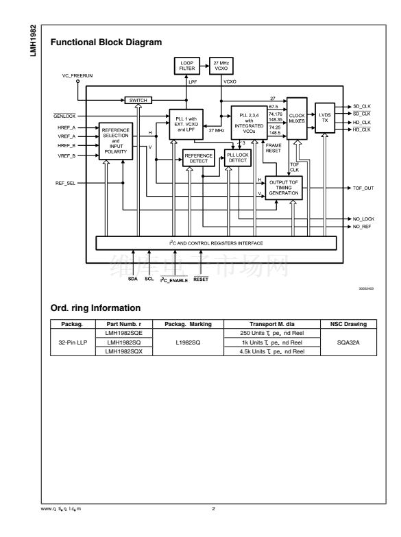
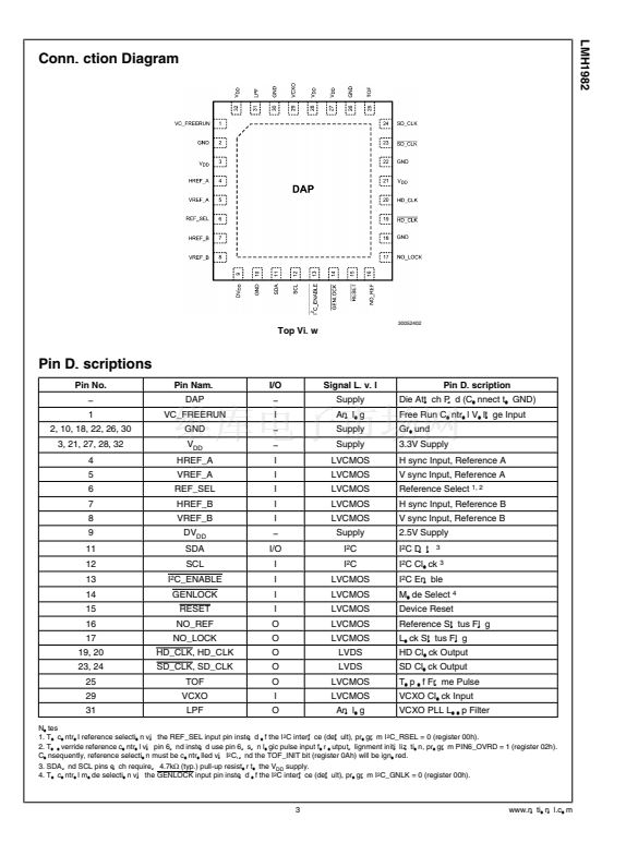
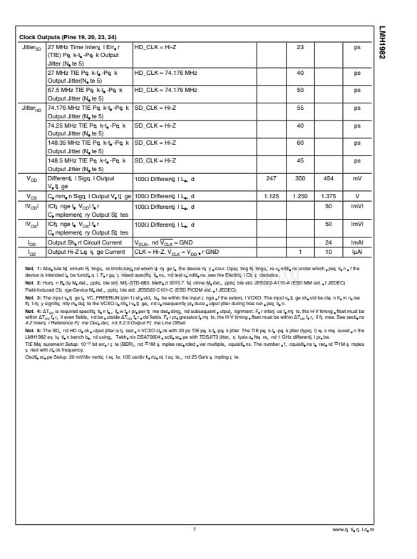
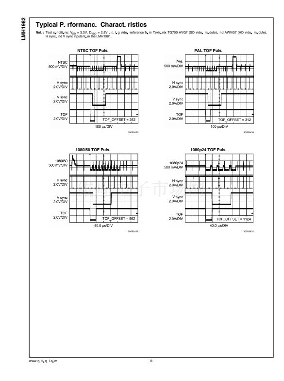
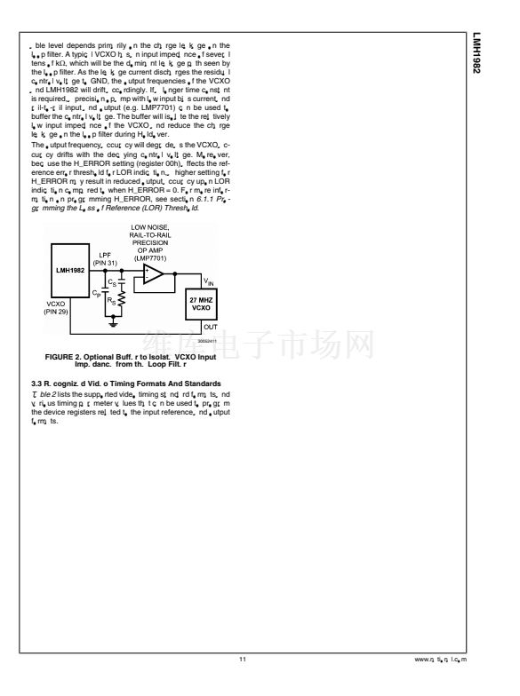
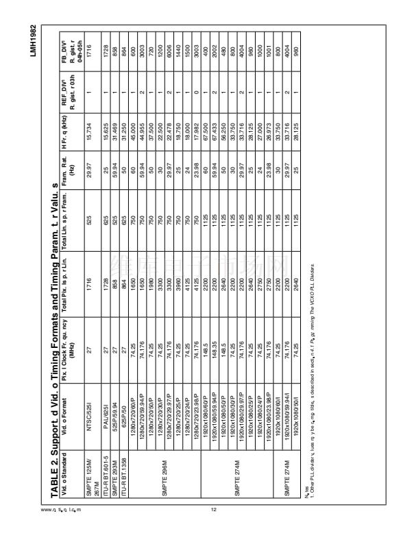
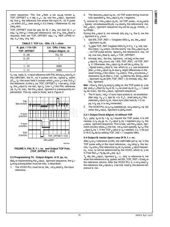
LMH1982
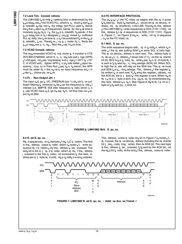
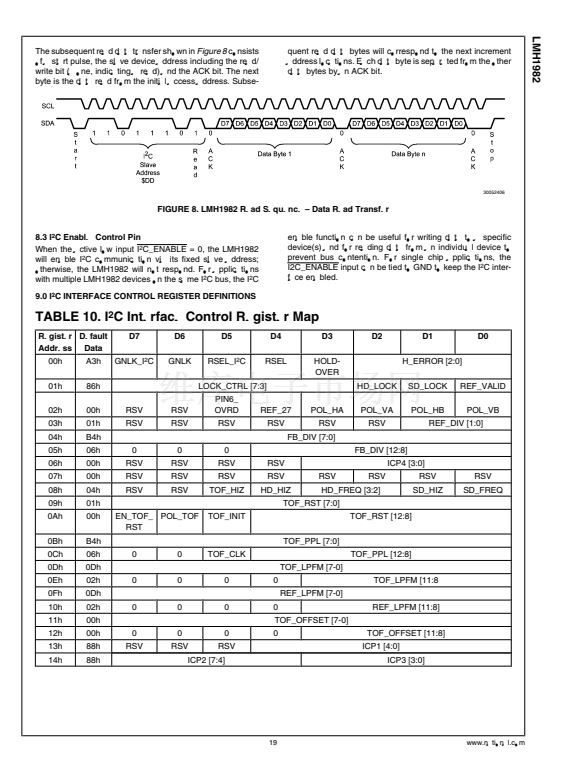
The subsequent read data transfer shown in
Figure 8
consists
of a start pulse, the slave device address including the read/
write bit (a one, indicating a read) and the ACK bit. The next
byte is the data read from the initial access address. Subse-
quent read data bytes will correspond to the next increment
address locations. Each data byte is separated from the other
data bytes by an ACK bit.
30052406
FIGURE 8. LMH1982 Read Sequence 鈥?Data Read Transfer
8.3 I
2
C Enable Control Pin
When the active low input I
2
C_ENABLE = 0, the LMH1982
will enable I
2
C communication via its fixed slave address;
otherwise, the LMH1982 will not respond. For applications
with multiple LMH1982 devices on the same I
2
C bus, the I
2
C
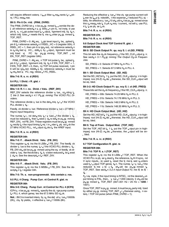
9.0 I
2
C INTERFACE CONTROL REGISTER DEFINITIONS
enable function can be useful for writing data to a specific
device(s) and for reading data from an individual device to
prevent bus contention. For single chip applications, the
I2C_ENABLE input can be tied to GND to keep the I
2
C inter-
face enabled.
TABLE 10. I
2
C Interface Control Register Map
Register Default
Address Data
00h
01h
02h
03h
04h
05h
06h
07h
08h
09h
0Ah
0Bh
0Ch
0Dh
0Eh
0Fh
10h
11h
12h
13h
14h
A3h
86h
00h
01h
B4h
06h
00h
00h
04h
01h
00h
B4h
06h
0Dh
02h
0Dh
02h
00h
00h
88h
88h
0
RSV
0
RSV
0
RSV
ICP2 [7:4]
0
0
0
0
TOF_OFFSET [7-0]
0
TOF_OFFSET [11:8]
ICP1 [4:0]
ICP3 [3:0]
0
0
0
0
REF_LPFM [7-0]
REF_LPFM [11:8]
0
0
TOF_CLK
TOF_LPFM [7-0]
TOF_LPFM [11:8
EN_TOF_ POL_TOF
RST
TOF_INIT
TOF_PPL [7:0]
TOF_PPL [12:8]
0
RSV
RSV
RSV
0
RSV
RSV
RSV
0
RSV
RSV
TOF_HIZ
RSV
RSV
HD_HIZ
RSV
RSV
HD_FREQ [3:2]
TOF_RST [12:8]
RSV
RSV
RSV
RSV
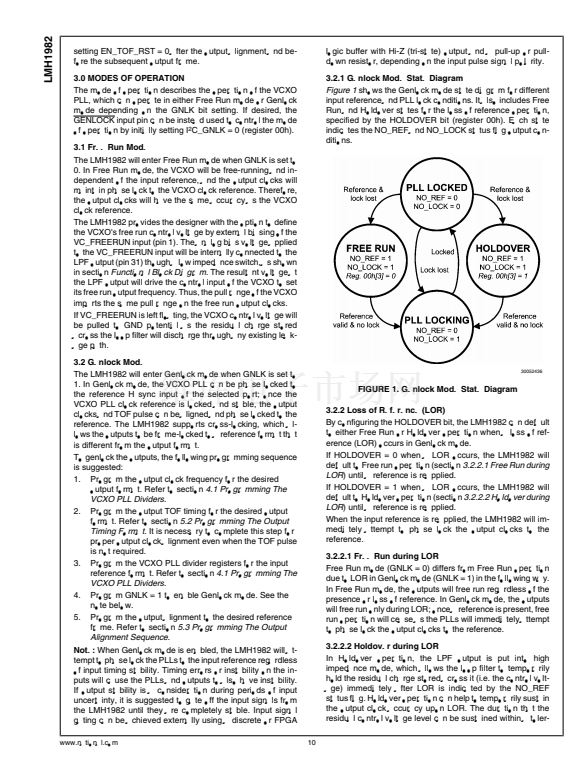
D7
GNLK_I
2
C
D6
GNLK
D5
RSEL_I
2
C
D4
RSEL
D3
HOLD-
OVER
HD_LOCK
POL_HA
RSV
FB_DIV [7:0]
FB_DIV [12:8]
ICP4 [3:0]
RSV
SD_HIZ
RSV
SD_FREQ
POL_VA
RSV
D2
D1
H_ERROR [2:0]
SD_LOCK
POL_HB
REF_VALID
POL_VB
D0
LOCK_CTRL [7:3]
PIN6_
OVRD
RSV
REF_27
RSV
REF_DIV [1:0]
TOF_RST [7:0]
19
www.national.com


 1
1
 2
2
 3
3
 4
4
 5
5
 6
6
 7
7
 8
8
 9
9
 10
10
 11
11
 12
12
 13
13
 14
14
 15
15
 16
16
 17
17
 18
18
 19
19
 20
20
 21
21
 22
22
 23
23
 24
24
 25
25
 26
26
 27
27
 28
28
