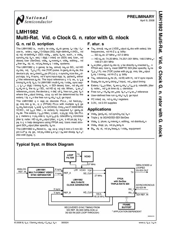
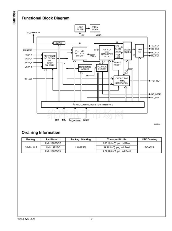
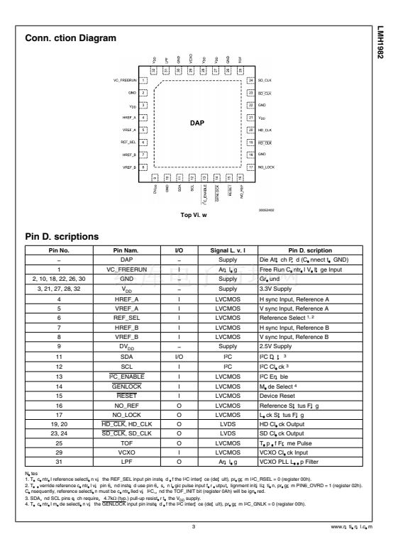
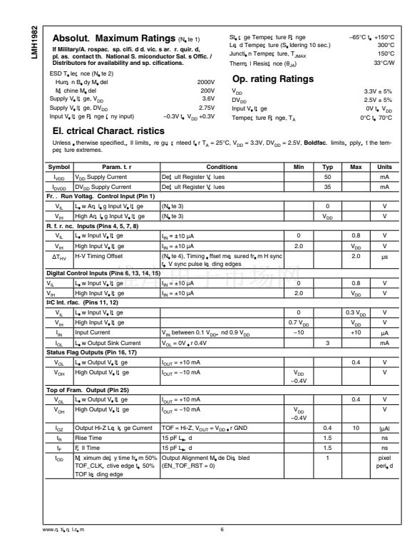
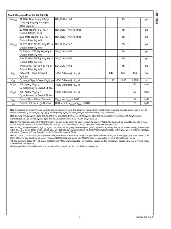
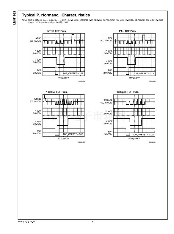
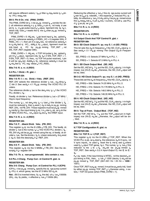
LMH1982
7.2 Lock Time Considerations
The LMH1982 lock time or settling time is determined by the
loop response of the VCXO PLL, which has a much lower loop
bandwidth compared to the integrated PLLs used to derive
the other output clock frequencies. Generally, the lock time is
inversely proportional to the loop bandwidth; however, if the
loop response is not designed or programmed for sufficient
PLL stability, the lock time may not be predicted from the loop
bandwidth alone. Therefore, any parameter that affects the
loop response can also affect the overall lock time.
7.3 VCXO Considerations
The recommended VCXO manufacturer part number is CTS
357LB3C27M0000, which has an absolute pull range (APR)
of 鹵50 ppm and operating temperature range of -20擄C to +70擄
C. A VCXO with a tighter APR can provide better output fre-
quency accuracy in Free Run operation; however, the APR
must be wider than the worst-case input frequency error in
order to achieve phase lock.
7.4 Free Run Output Jitter
The input voltage to VC_FREERUN (pin 1) should have suf-
ficient filtering to minimize noise over the frequency bands of
interest (i.e. SMPTE SDI jitter frequency bands) which can
cause VCXO input voltage modulation and thus free run out-
put clock jitter.
8.0 I
2
C INTERFACE PROTOCOL
The protocol of the I
2
C interface begins with the start pulse
followed by a byte comprised of a seven-bit slave device ad-
dress and a read/write bit as the LSB. Therefore, the address
of the LMH1982 for write sequences is DCh (1101 1100) and
the address for read sequences is DDh (1101 1101).
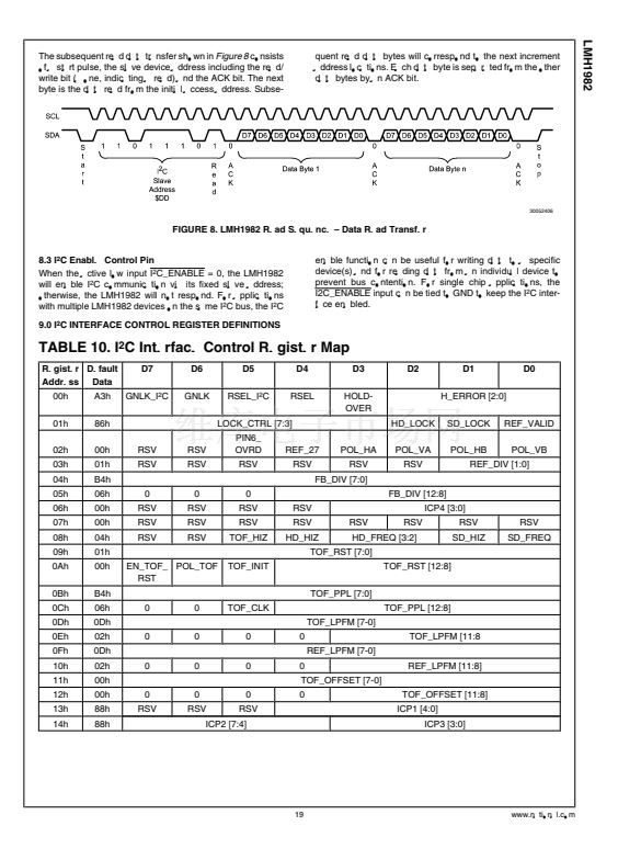
Figure
6, Figure 7,
and
Figure 8
show a write and read sequence
across the I
2
C interface.
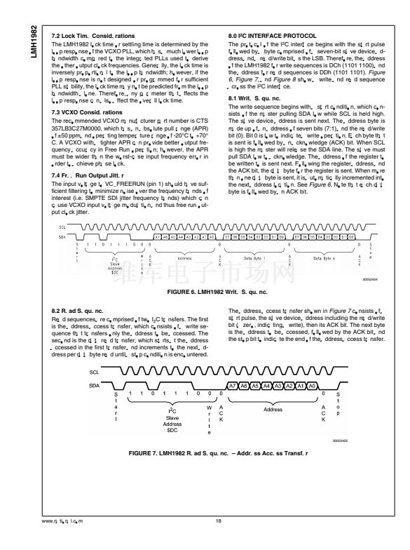
8.1 Write Sequence
The write sequence begins with a start condition, which con-
sists of the master pulling SDA low while SCL is held high.
The slave device address is sent next. The address byte is
made up of an address of seven bits (7:1) and the read/write
bit (0). Bit 0 is low to indicate a write operation. Each byte that
is sent is followed by an acknowledge (ACK) bit. When SCL
is high the master will release the SDA line. The slave must
pull SDA low to acknowledge. The address of the register to
be written to is sent next. Following the register address and
the ACK bit, the data byte for the register is sent. When more
than one data byte is sent, it is automatically incremented into
the next address location. See
Figure 6.
Note that each data
byte is followed by an ACK bit.
30052404
FIGURE 6. LMH1982 Write Sequence
8.2 Read Sequence
Read sequences are comprised of two I
2
C transfers. The first
is the address access transfer, which consists of a write se-
quence that transfers only the address to be accessed. The
second is the data read transfer, which starts at the address
accessed in the first transfer and increments to the next ad-
dress per data byte read until a stop condition is encountered.
The address access transfer shown in
Figure 7
consists of a
start pulse, the slave device address including the read/write
bit (a zero, indicating a write), then its ACK bit. The next byte
is the address to be accessed, followed by the ACK bit and
the stop bit to indicate the end of the address access transfer.
30052405
FIGURE 7. LMH1982 Read Sequence 鈥?Address Access Transfer
www.national.com
18


 1
1
 2
2
 3
3
 4
4
 5
5
 6
6
 7
7
 8
8
 9
9
 10
10
 11
11
 12
12
 13
13
 14
14
 15
15
 16
16
 17
17
 18
18
 19
19
 20
20
 21
21
 22
22
 23
23
 24
24
 25
25
 26
26
 27
27
 28
28
