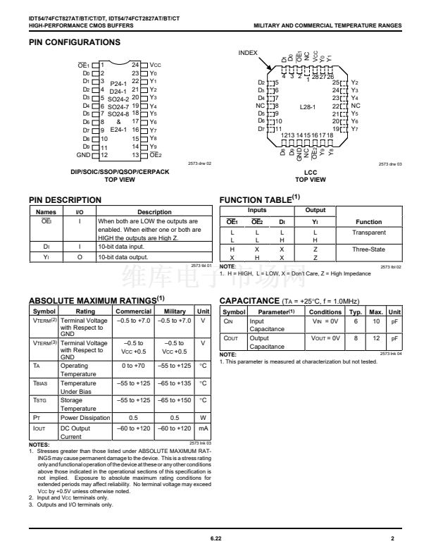
鈥?/div>
1.5
0.6
1.8
0.9
3.0
1.2
5.0
3.2
3.5
2.2
4.5
3.2
6.0
(5)
3.4
(5)
14.0
(5)
11.4
(5)
mA
V
IN
= GND FCT2827T
V
IN
= 3.4V
FCT827T
OE
1
=
OE
2
= GND
One Bit Toggling
V
CC
= Max.
Outputs Open
fi = 2.5MHz
50% Duty Cycle
V
IN
= GND FCT2827T
V
IN
= V
CC
FCT827T
V
IN
= GND FCT2827T
V
IN
= 3.4V
FCT827T
OE
1
=
OE
2
= GND
Eight Bits Toggling
V
IN
= GND FCT2827T
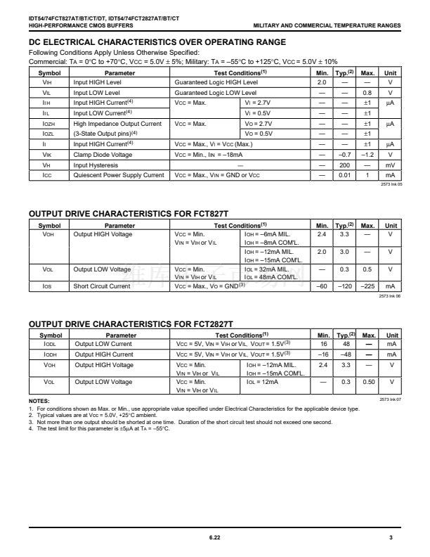
NOTES:
1. For conditions shown as Max. or Min., use appropriate value specified under Electrical Characteristics for the applicable device type.
2. Typical values are at V
CC
= 5.0V, +25擄C ambient.
3. Per TTL driven input (V
IN
= 3.4V). All other inputs at V
CC
or GND.
4. This parameter is not directly testable, but is derived for use in Total Power Supply Calculations.
5. Values for these conditions are examples of the I
CC
formula. These limits are guaranteed but not tested.
6. I
C
= I
QUIESCENT
+ I
INPUTS
+ I
DYNAMIC
I
C
= I
CC
+
鈭咺
CC
D
H
N
T
+ I
CCD
(f
CP/
2 + f
i
N
i
)
I
CC
= Quiescent Current
鈭咺
CC
= Power Supply Current for a TTL High Input (V
IN
= 3.4V)
D
H
= Duty Cycle for TTL Inputs High
N
T
= Number of TTL Inputs at D
H
I
CCD
= Dynamic Current Caused by an Input Transition Pair (HLH or LHL)
f
CP
= Clock Frequency for Register Devices (Zero for Non-Register Devices)
f
i
= Input Frequency
N
i
= Number of Inputs at f
i
All currents are in milliamps and all frequencies are in megahertz.
2573 tbl 08
6.22
4


 1
1
 2
2
 3
3
 4
4
 5
5
 6
6
 7
7
