IDT54/74FCT827AT/BT/CT/DT, IDT54/74FCT2827AT/BT/CT
HIGH-PERFORMANCE CMOS BUFFERS
MILITARY AND COMMERCIAL TEMPERATURE RANGES
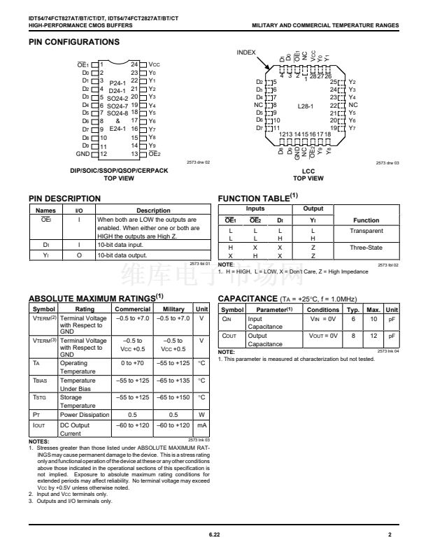
PIN CONFIGURATIONS
INDEX
2573 drw 02
D
8
D
9
GND
NC
OE
2
Y
9
Y
8
OE
1
D
0
D
1
D
2
D
3
D
4
D
5
D
6
D
7
D
8
D
9
GND
1
2
3 P24-1
4 D24-1
5 SO24-2
6 SO24-7
7 SO24-8
&
8
E24-1
9
10
11
12
24
23
22
21
20
19
18
17
16
15
14
13
V
CC
Y
0
Y
1
Y
2
Y
3
Y
4
Y
5
Y
6
Y
7
Y
8
Y
9
OE
2
D
2
D
3
D
4
NC
D
5
D
6
D
7
4 3 2
1 28 27 26
25
5
24
6
23
7
8
22
L28-1
9
21
20
10
19
11
1213 14 15 16 17 18
D
1
D
0
OE
1
NC
V
CC
Y
0
Y
1
Y
2
Y
3
Y
4
NC
Y
5
Y
6
Y
7
2573 drw 03
DIP/SOIC/SSOP/QSOP/CERPACK
TOP VIEW
LCC
TOP VIEW
PIN DESCRIPTION
Names
I/O
FUNCTION TABLE
(1)
Inputs
Output
D
I
L
H
X
X
Y
I
L
H
Z
Z
Function
Transparent
Three-State
2573 tbl 02
OE
I
D
I
Y
I
I
I
O
Description
When both are LOW the outputs are
enabled. When either one or both are
HIGH the outputs are High Z.
10-bit data input.
10-bit data output.
2573 tbl 01
OE
1
L
L
H
X
OE
2
L
L
X
H
NOTE:
1. H = HIGH, L = LOW, X = Don鈥檛 Care, Z = High Impedance
ABSOLUTE MAXIMUM RATINGS
(1)
Symbol
Rating
Commercial
V
TERM(2)
Terminal Voltage
鈥?.5 to +7.0
with Respect to
GND
V
TERM(3)
Terminal Voltage
鈥?.5 to
with Respect to
V
CC
+0.5
GND
T
A
Operating
0 to +70
Temperature
T
BIAS
Temperature
鈥?5 to +125
Under Bias
T
STG
Storage
鈥?5 to +125
Temperature
P
T
Power Dissipation
0.5
I
OUT
DC Output
Current
鈥?0 to +120
Military
鈥?.5 to +7.0
Unit
V
CAPACITANCE
(T
A
= +25擄C, f = 1.0MHz)
Symbol
Parameter
(1)
C
IN
Input
Capacitance
C
OUT
Output
Capacitance
Conditions
V
IN
= 0V
V
OUT
= 0V
Typ.
6
8
Max. Unit
10
pF
12
pF
2573 lnk 04
鈥?.5 to
V
CC
+0.5
鈥?5 to +125
鈥?5 to +135
鈥?5 to +150
0.5
鈥?0 to +120
V
擄C
擄C
擄C
W
mA
NOTE:
1. This parameter is measured at characterization but not tested.
2573 lnk 03
NOTES:
1. Stresses greater than those listed under ABSOLUTE MAXIMUM RAT-
INGS may cause permanent damage to the device. This is a stress rating
only and functional operation of the device at these or any other conditions
above those indicated in the operational sections of this specification is
not implied. Exposure to absolute maximum rating conditions for
extended periods may affect reliability. No terminal voltage may exceed
V
CC
by +0.5V unless otherwise noted.
2. Input and V
CC
terminals only.
3. Outputs and I/O terminals only.
6.22
2


 1
1
 2
2
 3
3
 4
4
 5
5
 6
6
 7
7
