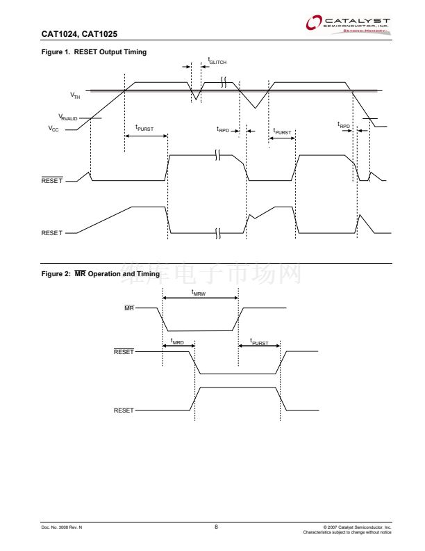
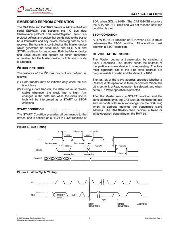
CAT1024, CAT1025
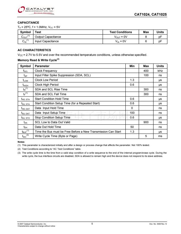
CAPACITANCE
T
A
= 25潞C, f = 1.0MHz, V
CC
= 5V
Symbol
C
OUT(1)
C
IN(1)
Test
Output Capacitance
Input Capacitance
Test Conditions
V
OUT
= 0V
V
IN
= 0V
Max
8
6
Units
pF
pF
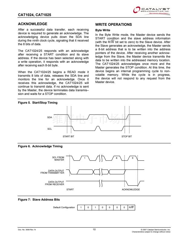
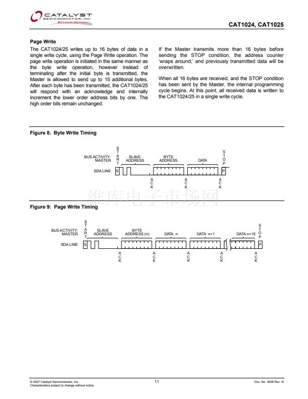
AC CHARACTERISTICS
V
CC
= 2.7V to 5.5V and over the recommended temperature conditions, unless otherwise specified.
Memory Read & Write Cycle
(2)
Symbol
f
SCL
t
SP
t
LOW
t
HIGH
t
R(1)
t
F(1)
t
HD; STA
t
SU; STA
t
HD; DAT
t
SU; DAT
t
SU; STO
t
AA
t
DH
t
BUF(1)
t
WC(3)
Parameter
Clock Frequency
Input Filter Spike Suppression (SDA, SCL)
Clock Low Period
Clock High Period
SDA and SCL Rise Time
SDA and SCL Fall Time
Start Condition Hold Time
Start Condition Setup Time (for a Repeated Start)
Data Input Hold Time
Data Input Setup Time
Stop Condition Setup Time
SCL Low to Data Out Valid
Data Out Hold Time
Time the Bus must be Free Before a New Transmission Can Start
Write Cycle Time (Byte or Page)
50
1.3
5
0.6
0.6
0
100
0.6
900
1.3
0.6
300
300
Min
Max
400
100
Units
kHz
ns
碌s
碌s
ns
ns
碌s
碌s
ns
ns
碌s
ns
ns
碌s
ms
Notes:
(1) This parameter is characterized initially and after a design or process change that affects the parameter. Not 100% tested.
(2) Test Conditions according to 鈥淎C Test Conditions鈥?table.
(3) The write cycle time is the time from a valid stop condition of a write sequence to the end of the internal program/erase cycle. During the
write cycle, the bus interface circuits are disabled, SDA is allowed to remain high and the device does not respond to its slave address.
漏 2007 Catalyst Semiconductor, Inc.
Characteristics subject to change without notice
5
Doc. No. 3008 Rev. N


 1
1
 2
2
 3
3
 4
4
 5
5
 6
6
 7
7
 8
8
 9
9
 10
10
 11
11
 12
12
 13
13
 14
14
 15
15
 16
16
 17
17
 18
18
 19
19
 20
20
