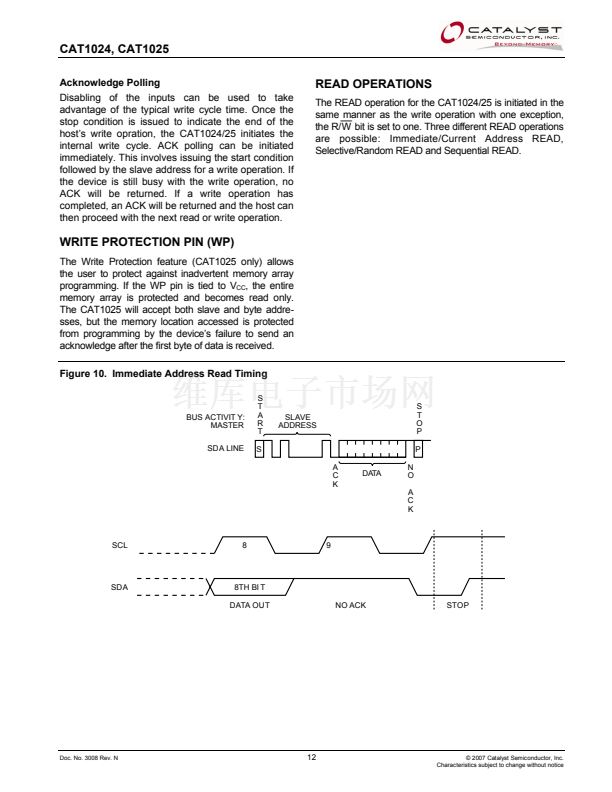
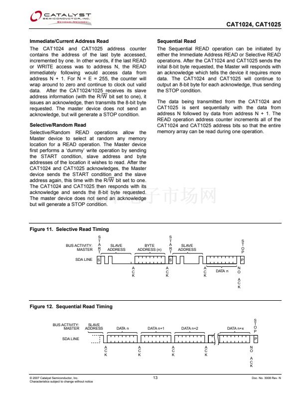
CAT1024, CAT1025
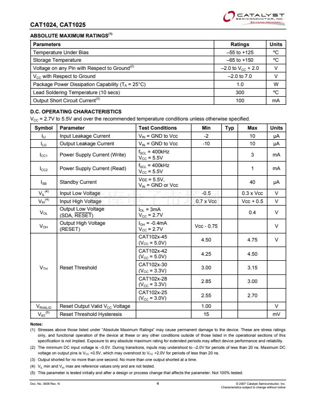
ABSOLUTE MAXIMUM RATINGS
(1)
Parameters
Temperature Under Bias
Storage Temperature
Voltage on any Pin with Respect to Ground
(2)
V
CC
with Respect to Ground
Package Power Dissipation Capability (T
A
= 25擄C)
Lead Soldering Temperature (10 secs)
Output Short Circuit Current
(3)
Ratings
鈥?5 to +125
鈥?5 to +150
鈥?.0 to V
CC
+ 2.0
鈥?.0 to 7.0
1.0
300
100
Units
潞C
潞C
V
V
W
潞C
mA
D.C. OPERATING CHARACTERISTICS
V
CC
= 2.7V to 5.5V and over the recommended temperature conditions unless otherwise specified.
Symbol
I
LI
I
LO
I
CC1
I
CC2
I
SB
V
IL(4)
V
IH(4)
V
OL
V
OH
Parameter
Input Leakage Current
Output Leakage Current
Power Supply Current (Write)
Power Supply Current (Read)
Standby Current
Input Low Voltage
Input High Voltage
Output Low Voltage
爐爐爐爐爐爐
(SDA, RESET)
Output High Voltage
(RESET)
I
OL
= 3mA
V
CC
= 2.7V
I
OH
= -0.4mA
V
CC
= 2.7V
CAT102x-45
(V
CC
= 5.0V)
CAT102x-42
(V
CC
= 5.0V)
V
TH
Reset Threshold
CAT102x-30
(V
CC
= 3.3V)
CAT102x-28
(V
CC
= 3.3V)
CAT102x-25
(V
CC
= 3.0V)
V
RVALID
V
RT
(5)
Test Conditions
V
IN
= GND to Vcc
V
IN
= GND to Vcc
f
SCL
= 400kHz
V
CC
= 5.5V
f
SCL
= 400kHz
V
CC
= 5.5V
Vcc = 5.5V,
V
IN
= GND or Vcc
Min
-2
-10
Typ
Max
10
10
3
1
40
Units
碌A(chǔ)
碌A(chǔ)
mA
mA
碌A(chǔ)
V
V
V
V
-0.5
0.7 x Vcc
0.3 x Vcc
Vcc + 0.5
0.4
Vcc - 0.75
4.50
4.25
3.00
2.85
2.55
1.00
15
4.75
4.50
3.15
3.00
2.70
V
Reset Output Valid V
CC
Voltage
Reset Threshold Hysteresis
V
mV
Notes:
(1) Stresses above those listed under 鈥淎bsolute Maximum Ratings鈥?may cause permanent damage to the device. These are stress ratings
only, and functional operation of the device at these or any other conditions outside of those listed in the operational sections of this
specification is not implied. Exposure to any absolute maximum rating for extended periods may affect device performance and reliability.
(2) The minimum DC input voltage is 鈥?.5V. During transitions, inputs may undershoot to 鈥?.0V for periods of less than 20 ns. Maximum DC
voltage on output pins is V
CC
+0.5V, which may overshoot to V
CC
+2.0V for periods of less than 20 ns.
(3) Output shorted for no more than one second. No more than one output shorted at a time.
(4) V
IL
min and V
IH
max are reference values only and are not tested.
(5) This parameter is tested initially and after a design or process change that affects the parameter. Not 100% tested.
Doc. No. 3008 Rev. N
4
漏 2007 Catalyst Semiconductor, Inc.
Characteristics subject to change without notice


 1
1
 2
2
 3
3
 4
4
 5
5
 6
6
 7
7
 8
8
 9
9
 10
10
 11
11
 12
12
 13
13
 14
14
 15
15
 16
16
 17
17
 18
18
 19
19
 20
20
