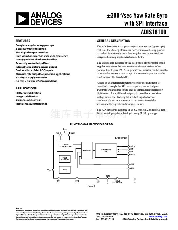
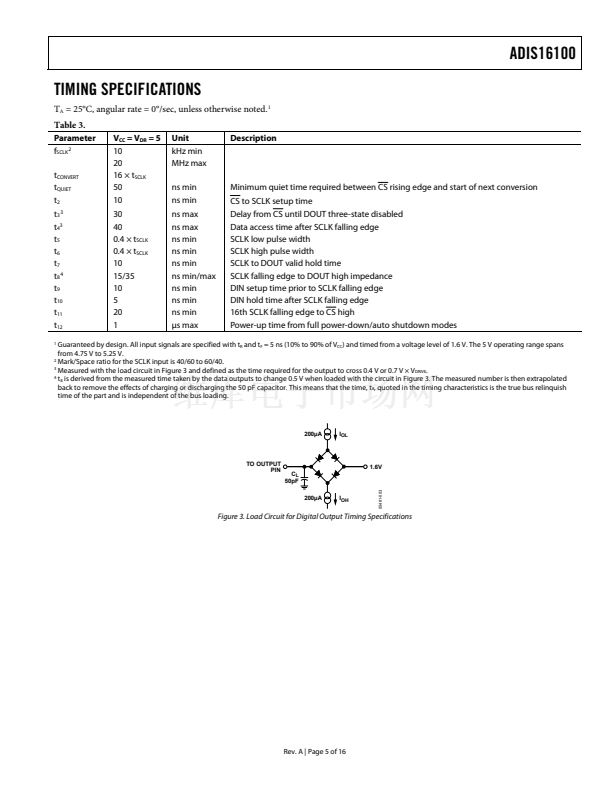
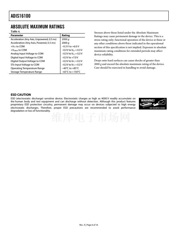
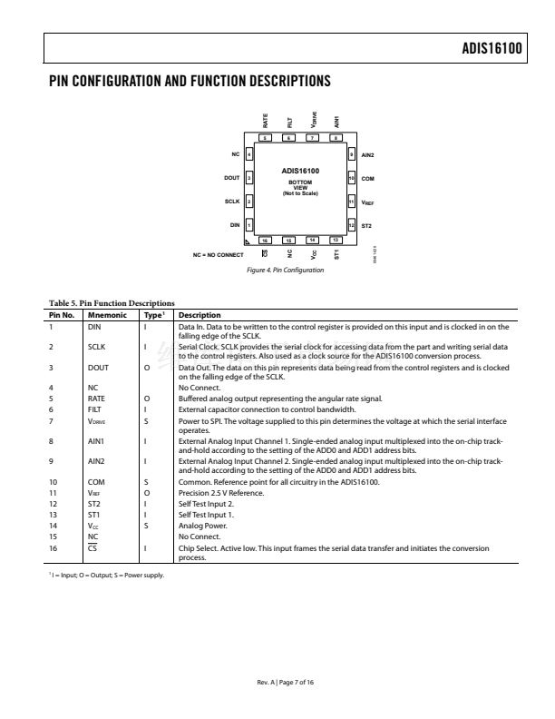
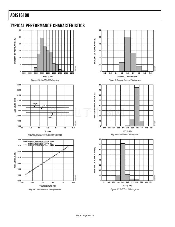
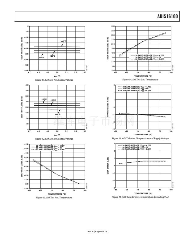
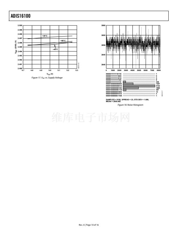
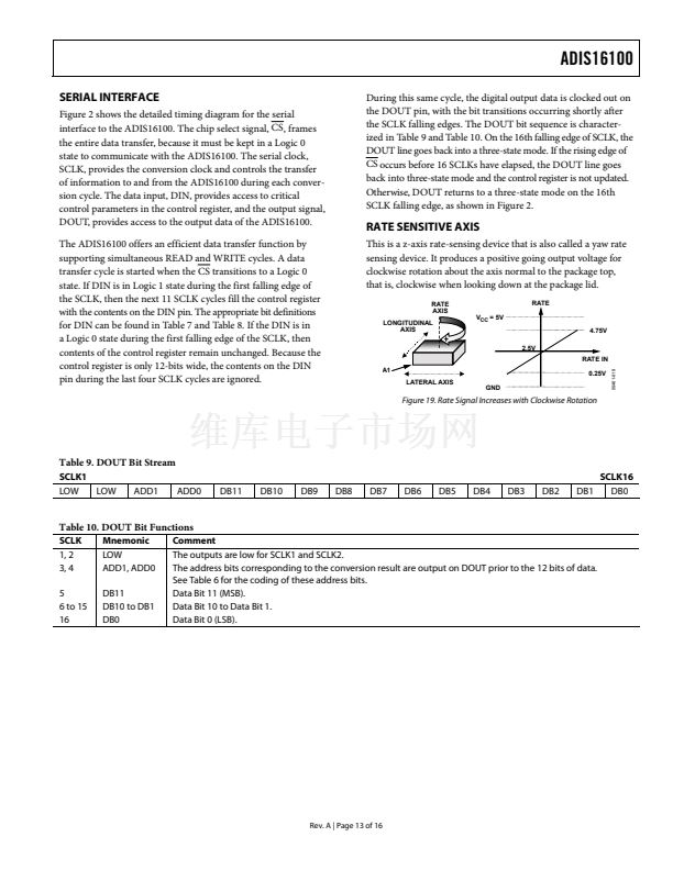
ADIS16100
SECOND-LEVEL ASSEMBLY
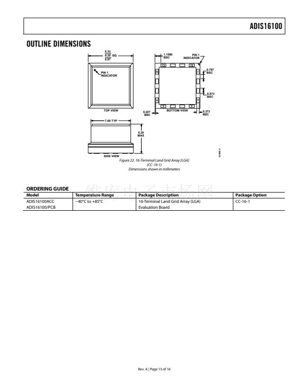
The recommended pad geometries for the ADIS16100 are
displayed in Figure 20. The ADIS16100 can be attached to
printed circuit boards using Sn63 or an equivalent solder.
Figure 21 and Table 11 provide recommended solder reflow
profiles for each solder type. Note: These profiles may not be
the optimum profile for the user鈥檚 application. In no case should
the temperature exceed 260擄C. It is recommended that the user
develop a reflow profile based upon the specific application.
In general, keep in mind that the lowest peak temperature and
shortest dwell time above the melt temperature of the solder
results in less shock and stress to the product. In addition,
evaluating the cooling rate and peak temperature can result in
a more reliable assembly.
6.873
2脳
0.5 BSC
16脳
T
P
RAMP-UP
CRITICAL ZONE
T
L
TO T
P
t
P
TEMPERATURE
T
L
T
SMAX
T
SMIN
t
L
t
S
PREHEAT
RAMP-DOWN
05461-022
t
25擄C TO PEAK
TIME
Figure 21. Recommended Solder Reflow Profiles
Table 11. Solder Profile Characteristics
Profile Feature
Average Ramp Rate (T
L
to T
P
)
Preheat
Minimum Temperature (T
SMIN
)
Maximum Temperature (T
SMAX
)
Time (T
SMIN
to T
SMAX
) (t
S
)
T
SMAX
to T
L
Ramp-Up Rate
Time Maintained Above Liquidous (T
L
)
Liquidous Temperature (T
L
)
Time (t
L
)
Peak Temperature (T
P
)
Time Within 5擄C of Actual Peak
Temperature (t
p
)
Ramp-Down Rate
Time 25擄C to Peak Temperature
Sn63/Pb37
3擄C/sec max
100擄C
150擄C
60 sec to 120 sec
3擄C/sec
183擄C
60 sec to 150 sec
240擄C + 0擄C/鈥?擄C
10 sec to 30 sec
6擄C/sec max
6 min max
0.67 BSC
12脳
1 BSC
16脳
0.9315
4脳
Figure 20. Second Level Assembly Pad Layout
Rev. A | Page 14 of 16
05461-018
0.9315
4脳


 1
1
 2
2
 3
3
 4
4
 5
5
 6
6
 7
7
 8
8
 9
9
 10
10
 11
11
 12
12
 13
13
 14
14
 15
15
 16
16
