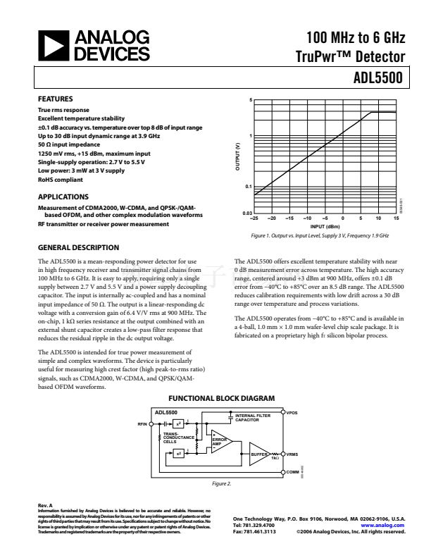
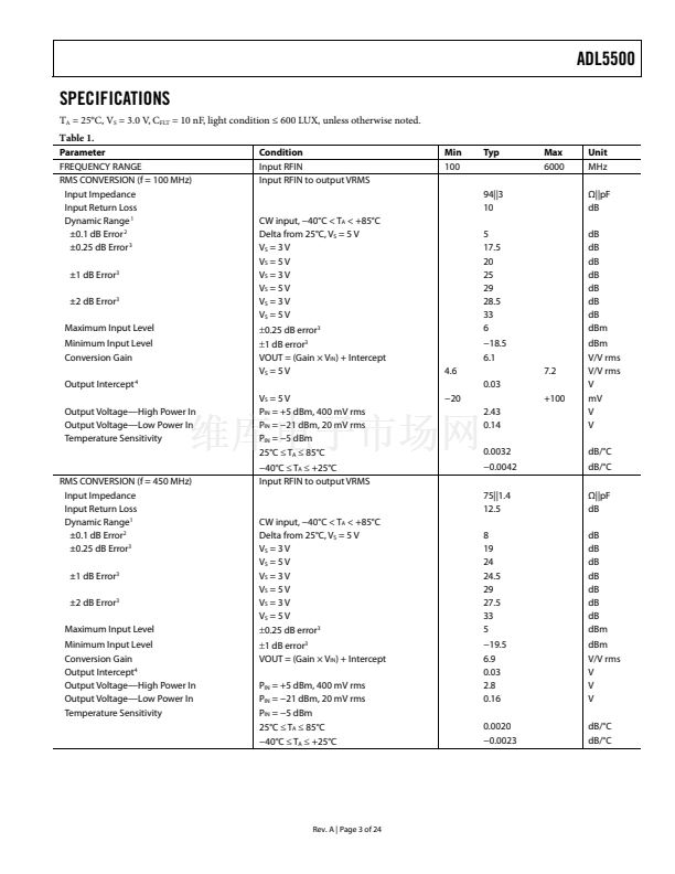
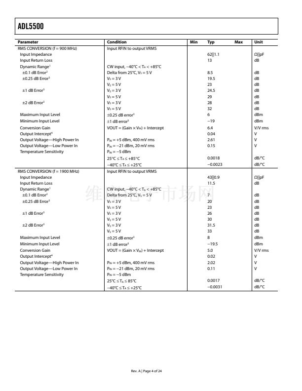
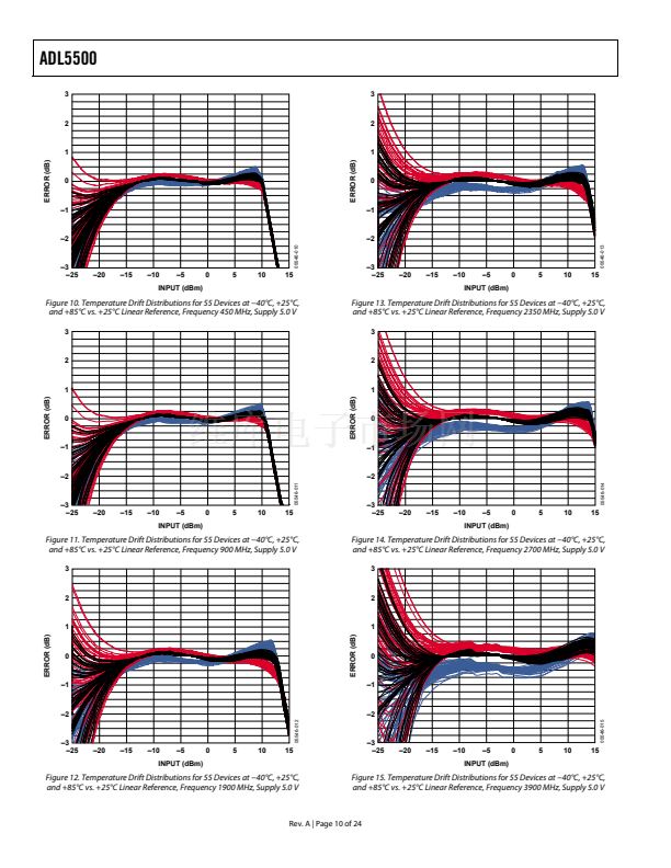
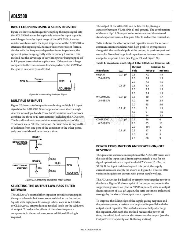
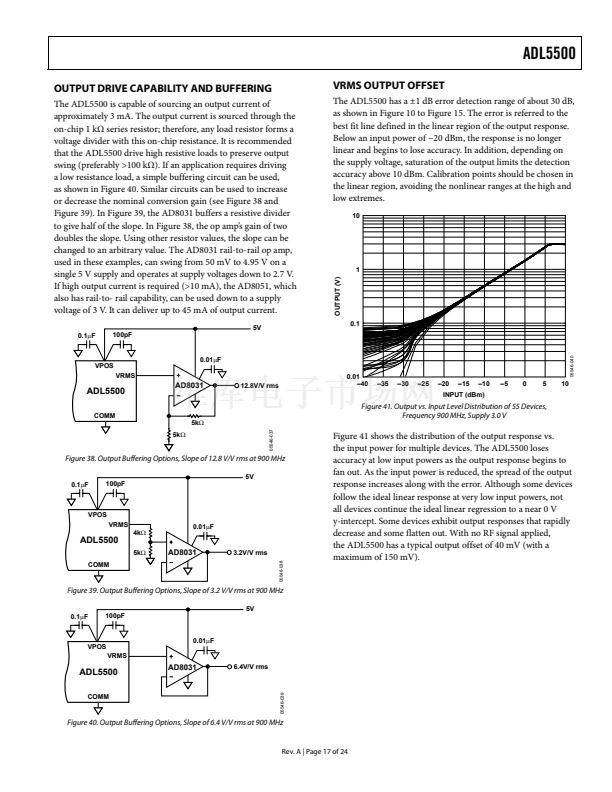
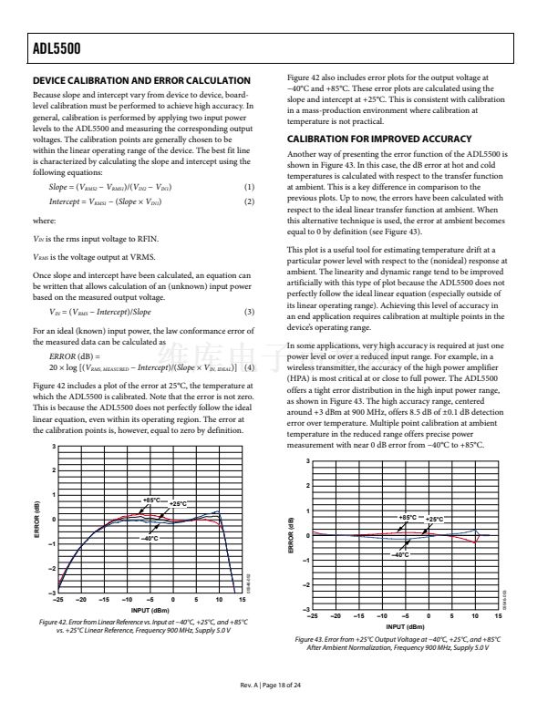
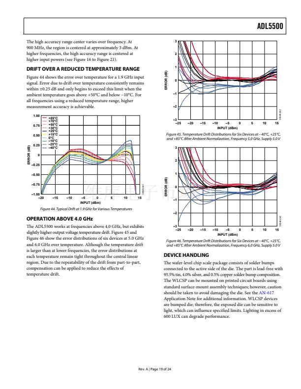
ADL5500
EVALUATION BOARD
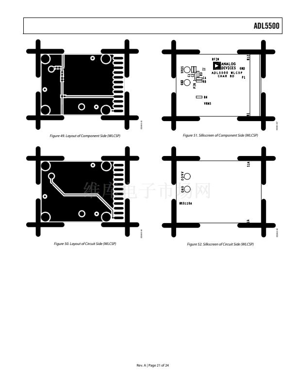
Figure 48 shows the schematic of the ADL5500 evaluation
board. The layout and silkscreen of the evaluation board layers
are shown in Figure 49 to Figure 52. The board is powered by a
single supply in the 2.7 V to 5.5 V range. The power supply is
decoupled by 100 pF and 0.01 渭F capacitors. Table 5 details the
various configuration options of the evaluation board.
Problems caused by impedance mismatch can arise using the
evaluation board to examine the ADL5500 performance. One
way to reduce these problems is to put a coaxial 3 dB attenuator
on the RFIN SMA connector. Mismatches at the source, cable,
and cable interconnection, as well as those occurring on the
evaluation board, can cause these problems.
A simple (and common) example of such a problem is triple
travel due to mismatch at both the source and the evaluation
board. Here the signal from the source reaches the evaluation
board and mismatch causes a reflection. When that reflection
reaches the source mismatch, it causes a new reflection, which
travels back to the evaluation board, adding to the original
signal incident at the board. The resultant voltage varies with
both cable length and frequency dependence on the relative
phase of the initial and reflected signals. Placing the 3 dB pad at
the input of the board improves the match at the board and thus
reduces the sensitivity to mismatches at the source. When such
precautions are taken, measurements are less sensitive to cable
length and other fixture issues. In an actual application when
the distance between ADL5500 and source is short and well-
defined, this 3 dB attenuator is not needed.
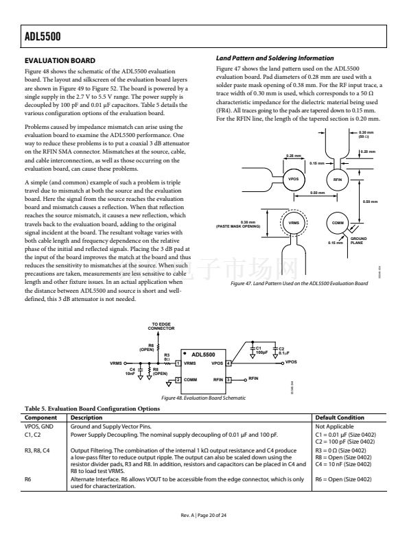
Land Pattern and Soldering Information
Figure 47 shows the land pattern used on the ADL5500
evaluation board. Pad diameters of 0.28 mm are used with a
solder paste mask opening of 0.38 mm. For the RF input trace, a
trace width of 0.30 mm is used, which corresponds to a 50 惟
characteristic impedance for the dielectric material being used
(FR4). All traces going to the pads are tapered down to 0.15 mm.
For the RFIN line, the length of the tapered section is 0.20 mm.
0.30 mm
(50
惟)
0.20 mm
0.28 mm
0.15 mm
VPOS
RFIN
0.50 mm
0.50 mm
0.38 mm
(PASTE MASK OPENING)
VRMS
COMM
0.15 mm
GROUND
PLANE
Figure 47. Land Pattern Used on the ADL5500 Evaluation Board
TO EDGE
CONNECTOR
R6
(OPEN)
R3
0惟
VRMS
C4
10nF
R8
(OPEN)
1
ADL5500
VRMS
VPOS
4
C1
100pF
C2
0.1渭F
VPOS
Figure 48. Evaluation Board Schematic
Table 5. Evaluation Board Configuration Options
Component
VPOS, GND
C1, C2
R3, R8, C4
Description
Ground and Supply Vector Pins.
Power Supply Decoupling. The nominal supply decoupling of 0.01 渭F and 100 pF.
Output Filtering. The combination of the internal 1 k惟 output resistance and C4 produce
a low-pass filter to reduce output ripple. The output can also be scaled down using the
resistor divider pads, R3 and R8. In addition, resistors and capacitors can be placed in C4 and
R8 to load test VRMS.
Alternate Interface. R6 allows VOUT to be accessible from the edge connector, which is only
used for characterization.
Default Condition
Not Applicable
C1 = 0.01 渭F (Size 0402)
C2 = 100 pF (Size 0402)
R3 = 0 惟 (Size 0402)
R8 = Open (Size 0402)
C4 = 10 nF (Size 0402)
R6 = Open (Size 0402)
R6
Rev. A | Page 20 of 24
05546-044
2
COMM
RFIN
3
RFIN
05546-054


 1
1
 2
2
 3
3
 4
4
 5
5
 6
6
 7
7
 8
8
 9
9
 10
10
 11
11
 12
12
 13
13
 14
14
 15
15
 16
16
 17
17
 18
18
 19
19
 20
20
 21
21
 22
22
 23
23
 24
24
