100 MHz to 6 GHz
TruPwr鈩?Detector
ADL5500
FEATURES
True rms response
Excellent temperature stability
鹵0.1 dB accuracy vs. temperature over top 8 dB of input range
Up to 30 dB input dynamic range at 3.9 GHz
50 惟 input impedance
1250 mV rms, +15 dBm, maximum input
Single-supply operation: 2.7 V to 5.5 V
Low power: 3 mW at 3 V supply
RoHS compliant
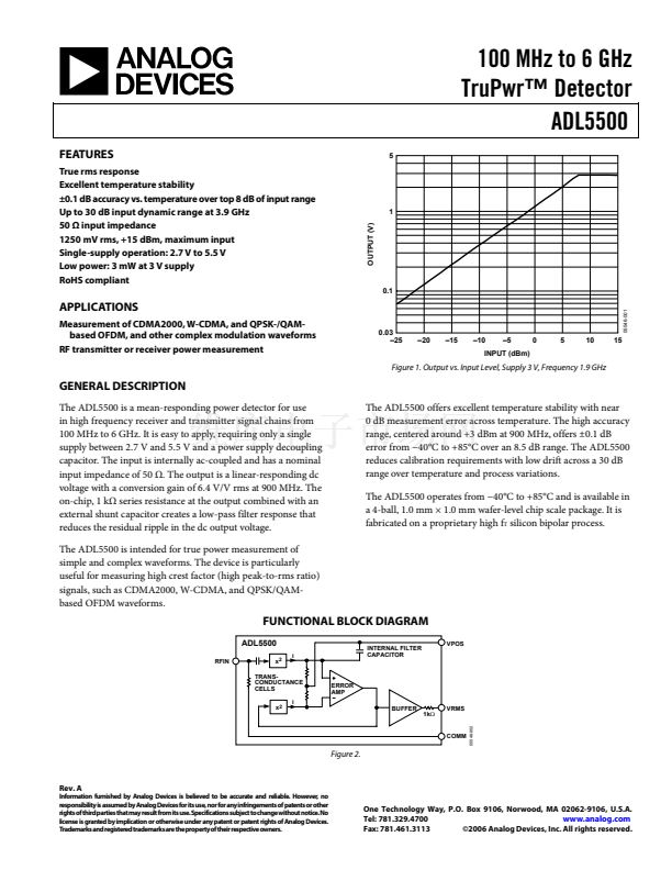
5
1
OUTPUT (V)
0.1
05546-001
APPLICATIONS
Measurement of CDMA2000, W-CDMA, and QPSK-/QAM-
based OFDM, and other complex modulation waveforms
RF transmitter or receiver power measurement
0.03
鈥?5
鈥?0
鈥?5
鈥?0
鈥?
0
5
10
15
INPUT (dBm)
Figure 1. Output vs. Input Level, Supply 3 V, Frequency 1.9 GHz
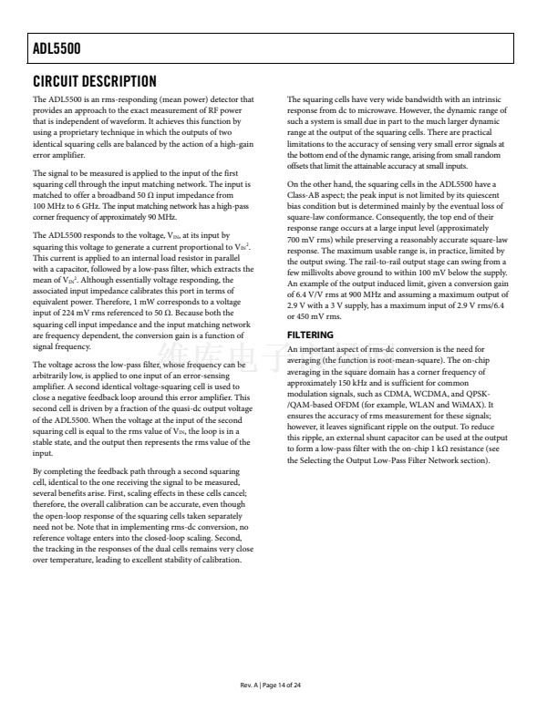
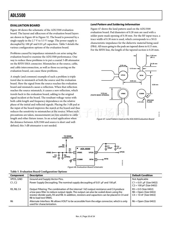
GENERAL DESCRIPTION
The ADL5500 is a mean-responding power detector for use
in high frequency receiver and transmitter signal chains from
100 MHz to 6 GHz. It is easy to apply, requiring only a single
supply between 2.7 V and 5.5 V and a power supply decoupling
capacitor. The input is internally ac-coupled and has a nominal
input impedance of 50 惟. The output is a linear-responding dc
voltage with a conversion gain of 6.4 V/V rms at 900 MHz. The
on-chip, 1 k惟 series resistance at the output combined with an
external shunt capacitor creates a low-pass filter response that
reduces the residual ripple in the dc output voltage.
The ADL5500 is intended for true power measurement of
simple and complex waveforms. The device is particularly
useful for measuring high crest factor (high peak-to-rms ratio)
signals, such as CDMA2000, W-CDMA, and QPSK/QAM-
based OFDM waveforms.
The ADL5500 offers excellent temperature stability with near
0 dB measurement error across temperature. The high accuracy
range, centered around +3 dBm at 900 MHz, offers 鹵0.1 dB
error from 鈭?0擄C to +85擄C over an 8.5 dB range. The ADL5500
reduces calibration requirements with low drift across a 30 dB
range over temperature and process variations.
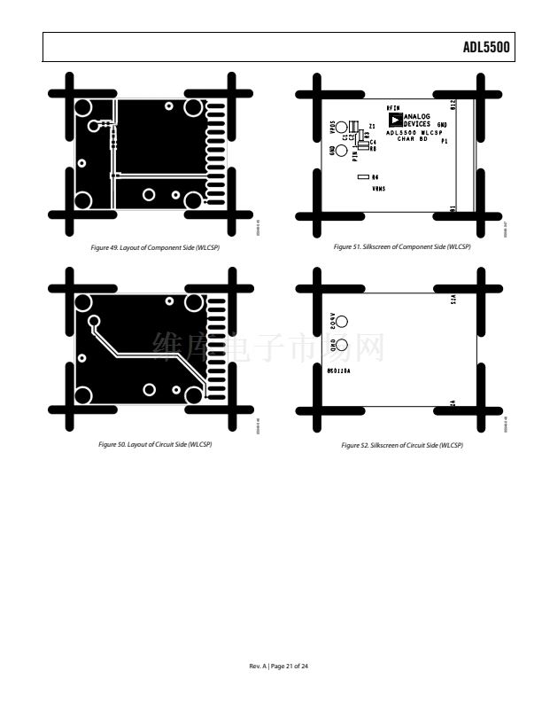
The ADL5500 operates from 鈭?0擄C to +85擄C and is available in
a 4-ball, 1.0 mm 脳 1.0 mm wafer-level chip scale package. It is
fabricated on a proprietary high f
T
silicon bipolar process.
FUNCTIONAL BLOCK DIAGRAM
ADL5500
RFIN
x
2
i
INTERNAL FILTER
CAPACITOR
VPOS
TRANS-
CONDUCTANCE
CELLS
x
2
i
ERROR
AMP
BUFFER
1k惟
05546-002
VRMS
COMM
Figure 2.
Rev. A
Information furnished by Analog Devices is believed to be accurate and reliable. However, no
responsibility is assumed by Analog Devices for its use, nor for any infringements of patents or other
rights of third parties that may result from its use. Specifications subject to change without notice. No
license is granted by implication or otherwise under any patent or patent rights of Analog Devices.
Trademarks and registered trademarks are the property of their respective owners.
One Technology Way, P.O. Box 9106, Norwood, MA 02062-9106, U.S.A.
Tel: 781.329.4700
www.analog.com
Fax: 781.461.3113
漏2006 Analog Devices, Inc. All rights reserved.


 1
1
 2
2
 3
3
 4
4
 5
5
 6
6
 7
7
 8
8
 9
9
 10
10
 11
11
 12
12
 13
13
 14
14
 15
15
 16
16
 17
17
 18
18
 19
19
 20
20
 21
21
 22
22
 23
23
 24
24
