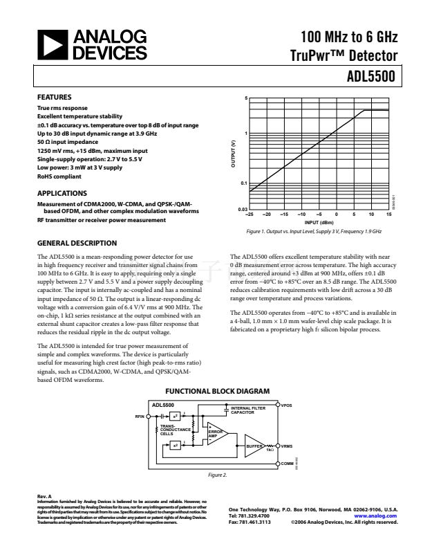
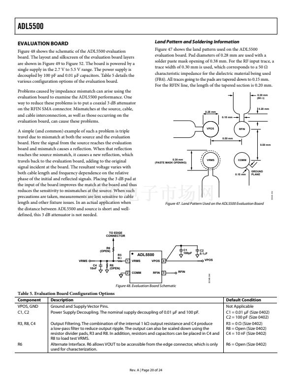
ADL5500
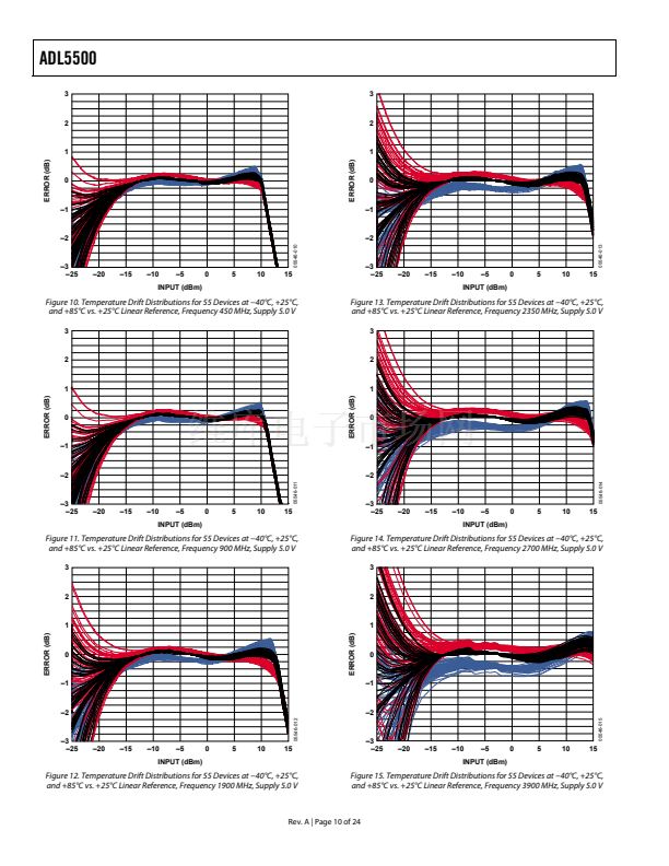
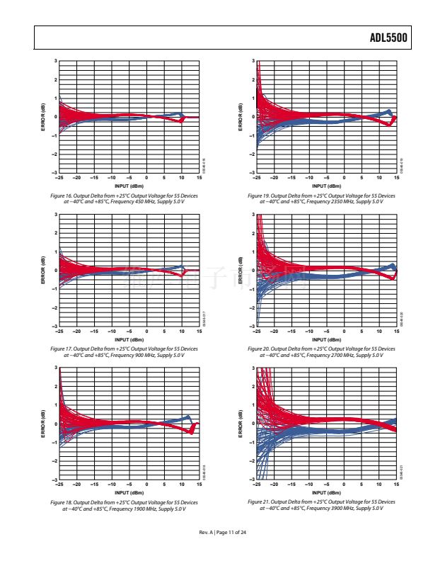
The high accuracy range center varies over frequency. At
900 MHz, the region is centered at approximately 3 dBm. At
higher frequencies, the high accuracy range is centered at
higher input powers (see Figure 16 to Figure 21).
ERROR (dB)
3
2
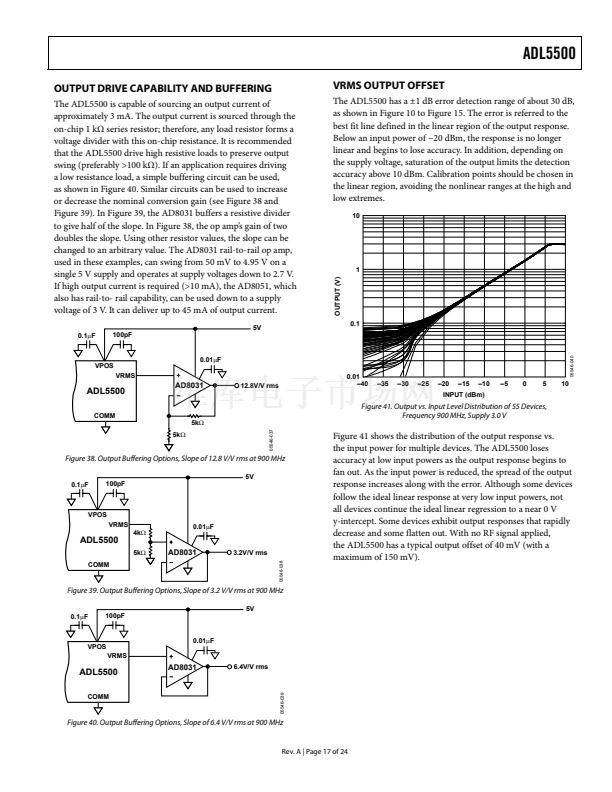
DRIFT OVER A REDUCED TEMPERATURE RANGE
Figure 44 shows the error over temperature for a 1.9 GHz input
signal. Error due to drift over temperature consistently remains
within 鹵0.25 dB and only begins to exceed this limit when the
ambient temperature goes above +50擄C and below 鈭?0擄C. For
all frequencies using a reduced temperature range, higher
measurement accuracy is achievable.
1.00
0.75
0.50
0.25
0
+85擄C
+70擄C
+50擄C
+30擄C
+25擄C
+15擄C
0擄C
鈥?0擄C
鈥?5擄C
鈥?0擄C
1
0
鈥?
鈥?
05546-042
鈥?
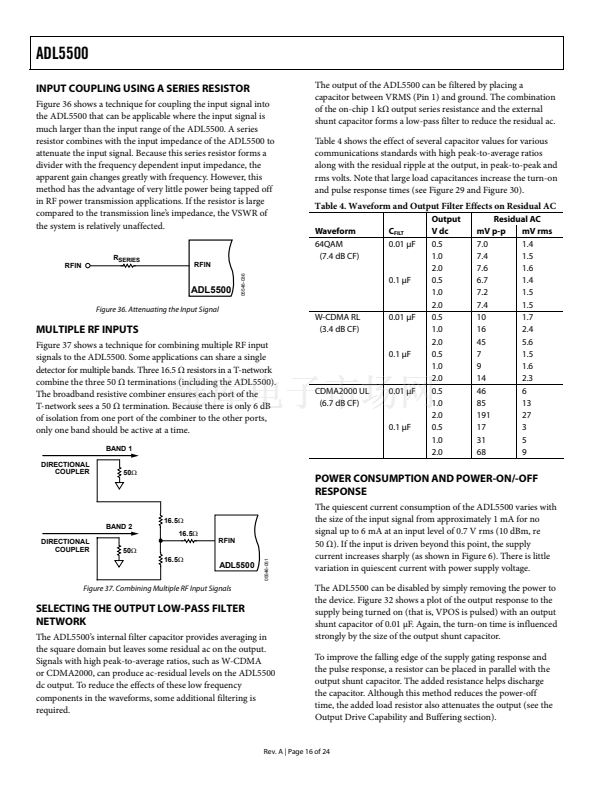
鈥?5
鈥?0
鈥?5
鈥?0
鈥?
0
5
10
15
INPUT (dBm)
Figure 45. Temperature Drift Distributions for Six Devices at 鈭?0擄C, +25擄C,
and +85擄C After Ambient Normalization, Frequency 5.0 GHz, Supply 5.0 V
3
ERROR (dB)
2
鈥?.25
鈥?.50
05546-041
1
鈥?.75
鈥?.00
鈥?0
ERROR (dB)
0
鈥?5
鈥?0
鈥?
0
5
10
15
INPUT (dBm)
鈥?
Figure 44. Typical Drift at 1.9 GHz for Various Temperatures
鈥?
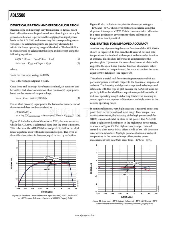
OPERATION ABOVE 4.0 GHz
The ADL5500 works at frequencies above 4.0 GHz, but exhibits
slightly higher output voltage temperature drift. Figure 45 and
Figure 46 show the error distributions of six devices at 5.0 GHz
and 6.0 GHz over temperature. Although the temperature drift
is larger than at lower frequencies, the error distributions at
each temperature remain tight throughout the central linear
region. Due to the repeatability of the drift from part-to-part,
compensation can be applied to reduce the effects of
temperature drift.
鈥?
鈥?5
鈥?0
鈥?5
鈥?0
鈥?
0
5
10
15
INPUT (dBm)
Figure 46. Temperature Drift Distributions for Six Devices at 鈭?0擄C, +25擄C,
and +85擄C After Ambient Normalization, Frequency 6.0 GHz, Supply 5.0 V
DEVICE HANDLING
The wafer-level chip scale package consists of solder bumps
connected to the active side of the die. The part is lead-free with
95.5% tin, 4.0% silver, and 0.5% copper solder bump composition.
The WLCSP can be mounted on printed circuit boards using
standard surface-mount assembly techniques; however, caution
should be taken to avoid damaging the die. See the
AN-617
Application Note for additional information. WLCSP devices
are bumped die; therefore, the exposed die can be sensitive to
light, which can influence specified limits. Lighting in excess of
600 LUX can degrade performance.
Rev. A | Page 19 of 24
05546-043


 1
1
 2
2
 3
3
 4
4
 5
5
 6
6
 7
7
 8
8
 9
9
 10
10
 11
11
 12
12
 13
13
 14
14
 15
15
 16
16
 17
17
 18
18
 19
19
 20
20
 21
21
 22
22
 23
23
 24
24
