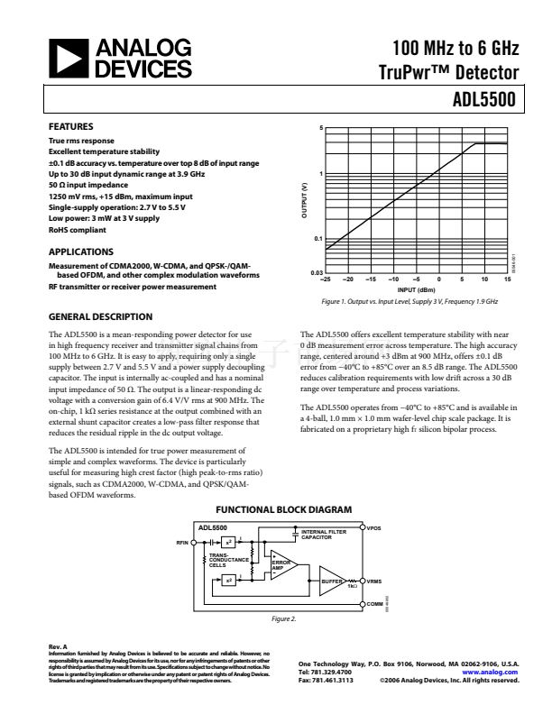
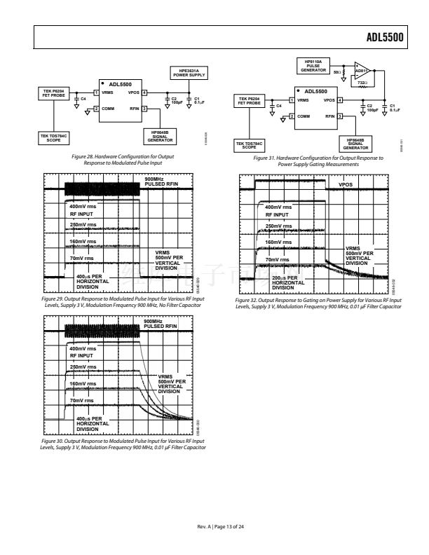
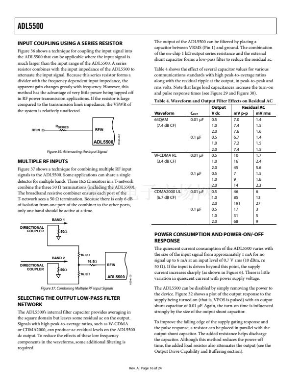
is the rms input voltage to RFIN.
is the voltage output at VRMS.
based on the measured output voltage.
鈭?/div>
Intercept)/Slope
(3)
(1)
(2)
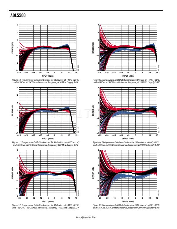
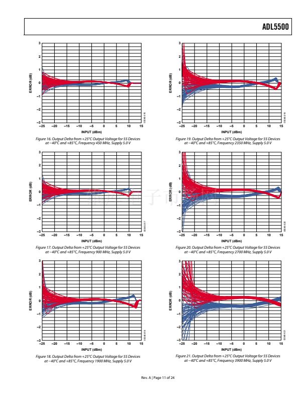
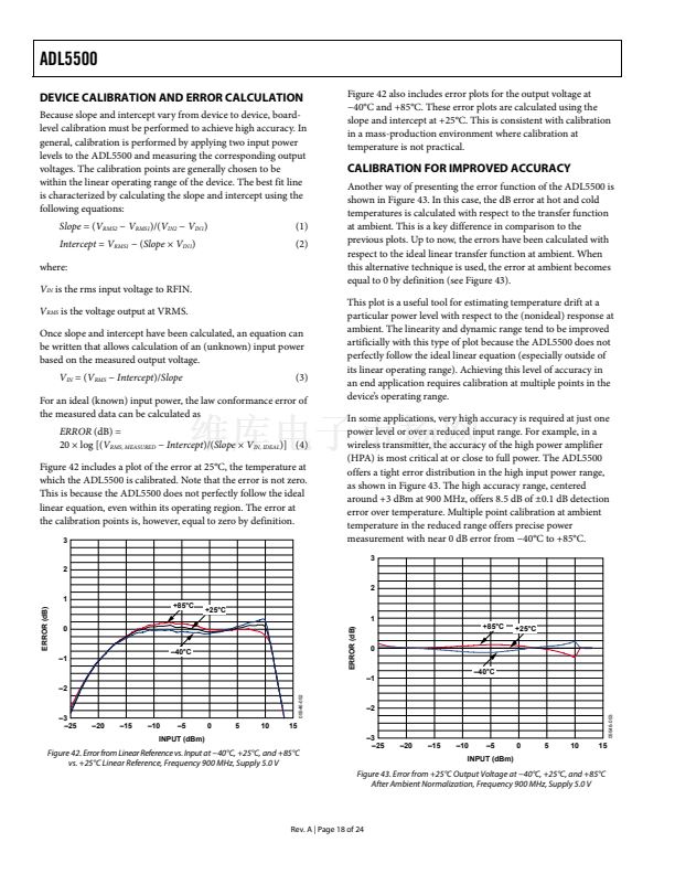
Figure 42 also includes error plots for the output voltage at
鈭?0擄C and +85擄C. These error plots are calculated using the
slope and intercept at +25擄C. This is consistent with calibration
in a mass-production environment where calibration at
temperature is not practical.
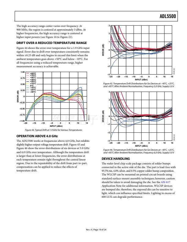
CALIBRATION FOR IMPROVED ACCURACY
Another way of presenting the error function of the ADL5500 is
shown in Figure 43. In this case, the dB error at hot and cold
temperatures is calculated with respect to the transfer function
at ambient. This is a key difference in comparison to the
previous plots. Up to now, the errors have been calculated with
respect to the ideal linear transfer function at ambient. When
this alternative technique is used, the error at ambient becomes
equal to 0 by definition (see Figure 43).
This plot is a useful tool for estimating temperature drift at a
particular power level with respect to the (nonideal) response at
ambient. The linearity and dynamic range tend to be improved
artificially with this type of plot because the ADL5500 does not
perfectly follow the ideal linear equation (especially outside of
its linear operating range). Achieving this level of accuracy in
an end application requires calibration at multiple points in the
device鈥檚 operating range.
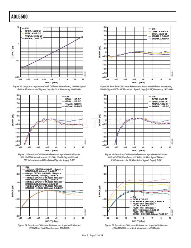
In some applications, very high accuracy is required at just one
power level or over a reduced input range. For example, in a
wireless transmitter, the accuracy of the high power amplifier
(HPA) is most critical at or close to full power. The ADL5500
offers a tight error distribution in the high input power range,
as shown in Figure 43. The high accuracy range, centered
around +3 dBm at 900 MHz, offers 8.5 dB of 鹵0.1 dB detection
error over temperature. Multiple point calibration at ambient
temperature in the reduced range offers precise power
measurement with near 0 dB error from 鈭?0擄C to +85擄C.
3
For an ideal (known) input power, the law conformance error of
the measured data can be calculated as
ERROR
(dB) =
20 脳 log [(V
RMS, MEASURED
鈭?/div>
Intercept)/(Slope
脳
V
IN, IDEAL
)] (4)
Figure 42 includes a plot of the error at 25擄C, the temperature at
which the ADL5500 is calibrated. Note that the error is not zero.
This is because the ADL5500 does not perfectly follow the ideal
linear equation, even within its operating region. The error at
the calibration points is, however, equal to zero by definition.
3
2
2
1
ERROR (dB)
+85擄C
+25擄C
1
0
鈥?0擄C
ERROR (dB)
+85擄C
0
鈥?0擄C
+25擄C
鈥?
鈥?
鈥?
05546-052
鈥?
05546-053
鈥?
鈥?5
鈥?0
鈥?5
鈥?0
鈥?
0
5
10
15
INPUT (dBm)
Figure 42. Error from Linear Reference vs. Input at 鈭?0擄C, +25擄C, and +85擄C
vs. +25擄C Linear Reference, Frequency 900 MHz, Supply 5.0 V
鈥?
鈥?5
鈥?0
鈥?5
鈥?0
鈥?
0
5
10
15
INPUT (dBm)
Figure 43. Error from +25擄C Output Voltage at 鈭?0擄C, +25擄C, and +85擄C
After Ambient Normalization, Frequency 900 MHz, Supply 5.0 V
Rev. A | Page 18 of 24


 1
1
 2
2
 3
3
 4
4
 5
5
 6
6
 7
7
 8
8
 9
9
 10
10
 11
11
 12
12
 13
13
 14
14
 15
15
 16
16
 17
17
 18
18
 19
19
 20
20
 21
21
 22
22
 23
23
 24
24
