Preliminary Technical Data
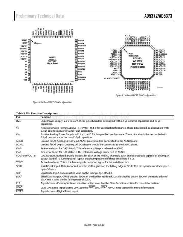
LDAC
VOUT26
VOUT25
VOUT24
DGND
VOUT7
AGND
DGND
DVCC
SDO
SDI
SCLK
SYNC
VOUT6
DVCC
AD5372/AD5373
CLR
64 63 62 61 60 59 58 57 56 55 54 53 52 51 50 49
RESET
1
BUSY
VOUT27
SIGGND3
VOUT28
VOUT29
2
3
4
5
6
48
PIN 1
IDENTIFIER
47
46
45
44
43
VOUT5
VOUT4
SIGGND0
VOUT3
VOUT2
VOUT30
7
VOUT31
8
NC
9
NC
10
NC
11
NC
12
NC
13
NC
14
AD5372
AD5373
TOP VIEW
(Not to Scale)
VOUT1
42
VOUT0
41
40
VREF0
VOUT23
39
VOUT22
37
36
35
34
33
38
VOUT21
VOUT20
VSS
VDD
SIGGND2
VOUT19
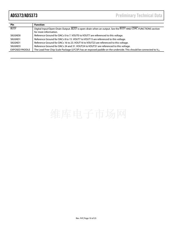
LDAC
CLR
RESET
BUSY
VOUT27
SIGGND3
VOUT28
VOUT29
VOUT30
VOUT31
NC
VDD
VSS
VREF1
1
2
3
4
5
6
7
8
9
10
11
12
13
14
56
55
54
53
52
51
50
49
48
47
46
45
44
43
VOUT26
VOUT25
VOUT24
AGND
DGND
DVCC
SDO
SDI
SCLK
SYNC
DVCC
DGND
VOUT7
VOUT6
PIN 1
INDICATOR
AD5372/
AD5373
TOP VIEW
(Not to scale)
42
41
40
39
38
37
36
35
34
33
32
31
30
29
VOUT5
VOUT4
SIGGND0
VOUT3
VOUT2
VOUT1
VOUT0
VREF0
VOUT23
VOUT22
VOUT21
VOUT20
VSS
VDD
NC
15
VDD
16
100605
NC = NO CONNECT
VOUT9 15
VOUT8 16
VOUT10 17
VOUT11 18
SIGGND1 19
VOUT12 20
VOUT13 21
VOUT14 22
VOUT15 23
VOUT16 24
VOUT17 25
VOUT18 26
VOU1T9 27
SIGGND2 28
17 18 19 20 21 22 23 24 25 26 27 28 29 30 31 32
VREF1
NC
NC
VOUT11
SIGGND1
VOUT9
VOUT10
VOUT12
VOUT13
VOUT14
VOUT15
VOUT16
VOUT17
VOUT18
VOUT8
VSS
5372-0060
Figure 7. 56-Lead LFCSP
Pin Configuration
Figure 6.64-Lead LQFP
Pin Configuration
Table 5. Pin Function Descriptions
Pin
DV
CC
V
SS
V
DD
AGND
DGND
V
REF
0
V
REF
1
VOUT0 to VOUT31
SYNC
1
SCLK
1
SDI
1
SDO
1
CLR
LDAC
RESET
Function
Logic Power Supply; 2.5 V to 5.5 V. These pins should be decoupled with 0.1 碌F ceramic capacitors and 10 碌F
capacitors.
Negative Analog Power Supply; 鈭?1.4 V to 鈭?6.5 V for specified performance. These pins should be decoupled with
0.1 碌F ceramic capacitors and 10 碌F capacitors.
Positive Analog Power Supply; +11.4 V to +16.5 V for specified performance. These pins should be decoupled with
0.1 碌F ceramic capacitors and 10 碌F capacitors.
Ground for All Analog Circuitry. All AGND pins should be connected to the AGND plane.
Ground for All Digital Circuitry. All DGND pins should be connected to the DGND plane.
Reference Input for DACs 0 to 7. This reference voltage is referred to AGND.
Reference Input for DACs 8 to 31. This reference voltage is referred to AGND.
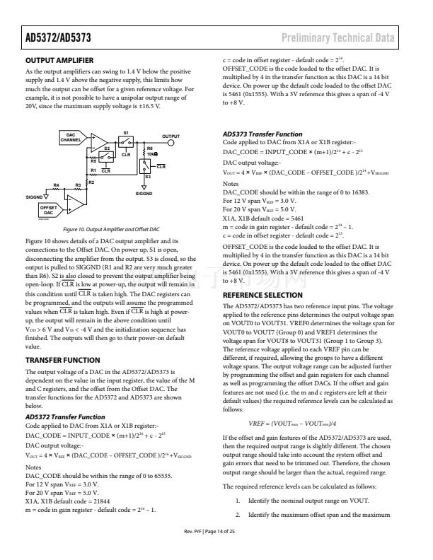
DAC Outputs. Buffered analog outputs for each of the 40 DAC channels. Each analog output is capable of driving an
output load of 10 k鈩?to ground. Typical output impedance of these amplifiers is 1 鈩?
Active Low Input. This is the frame synchronization signal for the serial interface.
Serial Clock Input. Data is clocked into the shift register on the falling edge of SCLK. This pin operates at clock speeds
up to 50 MHz.
Serial Data Input. Data must be valid on the falling edge of SCLK.
Serial Data Output. CMOS output. SDO can be used for readback. Data is clocked out on SDO on the rising edge of
SCLK and is valid on the falling edge of SCLK.
Asynchronous Clear Input (level sensitive, active low). See the Clear Function section for more information
Load DAC Logic Input (Active Low).See the BUSY AND LDAC FUNCTIONS section for more information.
Asynchronous Digital Reset Input.
Rev. PrF | Page 9 of 25


 1
1
 2
2
 3
3
 4
4
 5
5
 6
6
 7
7
 8
8
 9
9
 10
10
 11
11
 12
12
 13
13
 14
14
 15
15
 16
16
 17
17
 18
18
 19
19
 20
20
 21
21
 22
22
 23
23
 24
24
 25
25
