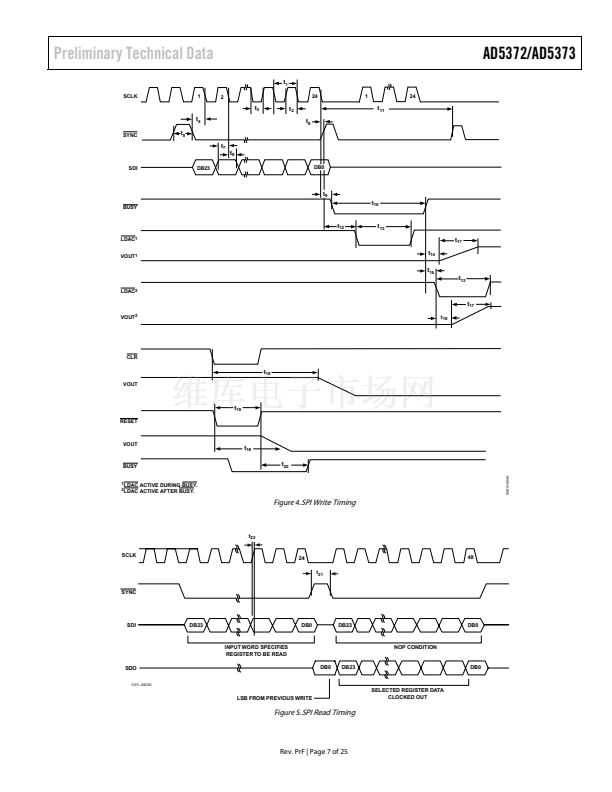
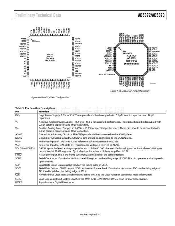
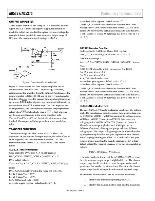
Preliminary Technical Data
FEATURES
32-channel DAC in 56-LFCSP and 64-LQFP
AD5372 Guaranteed monotonic to 16 bits
AD5373 Guaranteed monotonic to 14 bits
Maximum output voltage span of 4 脳 V
REF
(20 V)
Nominal output voltage range of -4 V to +8 V
Multiple, independent output spans available
System calibration function allowing user-programmable
offset and gain
Channel grouping and addressing features
Thermal Monitoring Function
DSP/microcontroller-compatible serial interface
2.5 V to 5.5 V JEDEC-compliant digital levels
DV
CC
V
DD
V
SS
32-Channel, 16/14, Serial Input,
Voltage-Output DACs
AD5372/AD5373
Power-on reset
Digital reset (RESET)
Clear function to user-defined SIGGND (CLR pin)
Simultaneous update of DAC outputs (LDAC pin)
APPLICATIONS
Level setting in automatic test equipment (ATE)
Variable optical attenuators (VOA)
Optical switches
Industrial control systems
Instrumentation
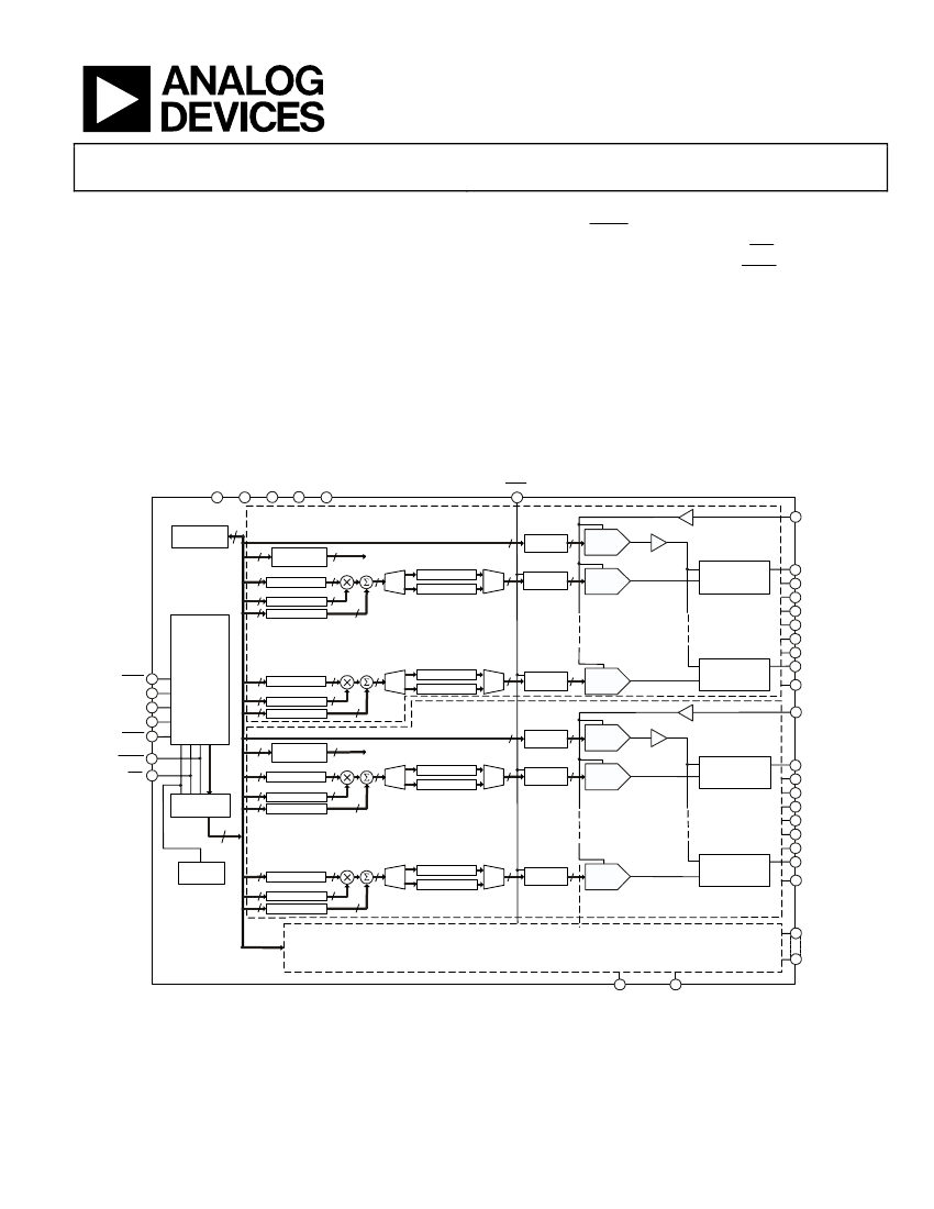
FUNCTIONAL BLOCK DIAGRAM
AGND DNGD
LDAC
VREF0
14
TO
MUX 2's
n
A/B
MUX
X2A REGISTER
X2B REGISTER
MUX n
2
n
OFS0
REGISTER
n
DAC 0
REGISTER
OFFSET
DAC 0
BUFFER
DAC 0
OUTPUT BUFFER
AND POWER
DOWN CONTROL
BUFFER
GROUP 0
CONTROL
REGISTER
n
8
n
n
n
n = 16 FOR AD5372
n = 14 FOR AD5373
A/B SELECT
REGISTER
X1 REGISTER
n
M REGISTER
C REGISTER
n
8
n
VOUT0
VOUT1
VOUT2
VOUT3
VOUT4
VOUT5
VOUT6
VOUT7
SIGGND0
路
路
路
路
路
路
SYNC
SDI
SCLK
SDO
BUSY
SERIAL
INTERFACE
n
n
n
n
n
路
路
路
路
路
路
n
路
路
路
路
路
路
n
路
路
路
路
路
路
A/B
MUX
路
路
路
路
路
路
X2A REGISTER
X2B REGISTER
X1 REGISTER
M REGISTER
C REGISTER
MUX n
2
路
路
路
路
路
路
n
DAC 7
REGISTER
路
路
路
路
路
路
路
路
路
路
路
路
DAC 7
路
路
路
路
路
路
OUTPUT BUFFER
AND POWER
DOWN CONTROL
GROUP 1
14
n
OFS1
REGISTER
n
DAC 0
REGISTER
OFFSET
DAC 1
BUFFER
X2A REGISTER
X2B REGISTER
MUX n
2
DAC 0
OUTPUT BUFFER
AND POWER
DOWN CONTROL
VREF1
8
RESET
CLR
STATE
MACHINE
n
n
n
n
A/B SELECT
REGISTER
X1 REGISTER
8
n
n
TO
MUX 2's
n
A/B
MUX
n
VOUT8
VOUT9
VOUT10
VOUT11
VOUT12
VOUT13
VOUT14
VOUT15
SIGGND1
M REGISTER
C REGISTER
路
路
路
路
路
路
POWER-ON
RESET
n
n
n
n
n
路
路
路
路
路
路
n
路
路
路
路
路
路
n
路
路
路
路
路
路
A/B
MUX
路
路
路
路
路
路
路
路
路
路
路
路
MUX n
2
X1 REGISTER
M REGISTER
C REGISTER
X2A REGISTER
X2B REGISTER
n
DAC 7
REGISTER
路
路
路
路
路
路
路
路
路
路
路
路
DAC 7
路
路
路
路
路
路
OUTPUT BUFFER
AND POWER
DOWN CONTROL
AD5372/
AD5373
VREF1 SUPPLIES
GROUP 1 TO 3
GROUP 2 TO GROUP 3
ARE IDENTICAL TO GROUP 1
VOUT16
TO
VOUT31
5372-0001B
SIGGND2
SIGGND3
Figure 1.
AD5372/AD5373鈥擯rotected by U.S. Patent No. 5,969,657; other patents pending
Rev. PrF
Information furnished by Analog Devices is believed to be accurate and reliable.
However, no responsibility is assumed by Analog Devices for its use, nor for any
infringements of patents or other rights of third parties that may result from its use.
Specifications subject to change without notice. No license is granted by implication
or otherwise under any patent or patent rights of Analog Devices. Trademarks and
registered trademarks are the property of their respective companies.
One Technology Way, P.O. Box 9106, Norwood, MA 02062-9106, U.S.A.
www.analog.com
Tel: 781.329.4700
Fax: 781.326.8703
漏 2006 Analog Devices, Inc. All rights reserved.


 1
1
 2
2
 3
3
 4
4
 5
5
 6
6
 7
7
 8
8
 9
9
 10
10
 11
11
 12
12
 13
13
 14
14
 15
15
 16
16
 17
17
 18
18
 19
19
 20
20
 21
21
 22
22
 23
23
 24
24
 25
25
