AD5372/AD5373
ABSOLUTE MAXIMUM RATINGS
T
A
= 25擄C, unless otherwise noted.
Transient currents of up to 100 mA do not cause SCR latch-up.
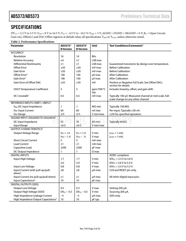
Table 4. Absolute Maximum Ratings
Parameter
V
DD
to AGND
V
SS
to AGND
DV
CC
to DGND
Digital Inputs to DGND
Digital Outputs to DGND
V
REF
1, V
REF
2 to AGND
VOUT0鈥揤OUT39 to AGND
SIGGND to AGND
AGND to DGND
Operating Temperature Range (T
A
)
Industrial (B Version)
Storage Temperature Range
Junction Temperature (T
J
max)
胃
JA
Thermal Impedance
56-LFCSP
64-LQFP
Reflow Soldering
Peak Temperature
Time at Peak Temperature
Rating
鈭?.3 V to +17 V
鈭?7 V to +0.3 V
鈭?.3 V to +7 V
鈭?.3 V to V
CC
+ 0.3 V
鈭?.3 V to V
CC
+ 0.3 V
鈭?.3 V to +7 V
V
SS
鈭?0.3 V to V
DD
+ 0.3 V
V
SS
鈭?0.3 V to V
DD
+ 0.3 V
鈭?.3 V to +0.3 V
鈭?0擄C to +85擄C
鈭?5擄C to +150擄C
130擄C
24擄C/w
45.5擄C/w
230擄C
10 s to 40 s
Preliminary Technical Data
Stresses above those listed under Absolute Maximum Ratings
may cause permanent damage to the device. This is a stress
rating only, and functional operation of the device at these or
any other conditions above those listed in the operational
sections of this specification is not implied. Exposure to
absolute maximum rating conditions for extended periods may
affect device reliability.
ESD CAUTION
ESD (electrostatic discharge) sensitive device. Electrostatic charges as high as 4000 V readily accumulate on
the human body and test equipment and can discharge without detection. Although this product features
proprietary ESD protection circuitry, permanent damage may occur on devices subjected to high energy
electrostatic discharges. Therefore, proper ESD precautions are recommended to avoid performance
degradation or loss of functionality.
Rev. PrF| Page 8 of 25


 1
1
 2
2
 3
3
 4
4
 5
5
 6
6
 7
7
 8
8
 9
9
 10
10
 11
11
 12
12
 13
13
 14
14
 15
15
 16
16
 17
17
 18
18
 19
19
 20
20
 21
21
 22
22
 23
23
 24
24
 25
25
