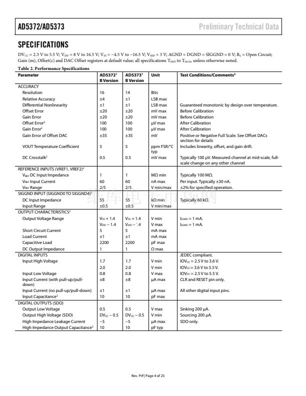
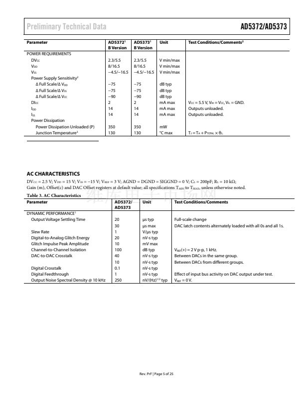
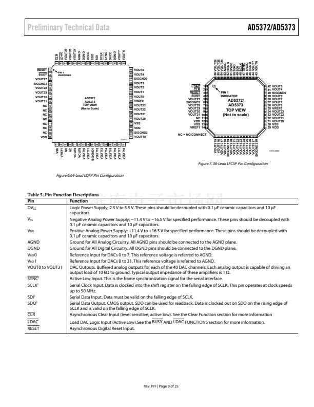
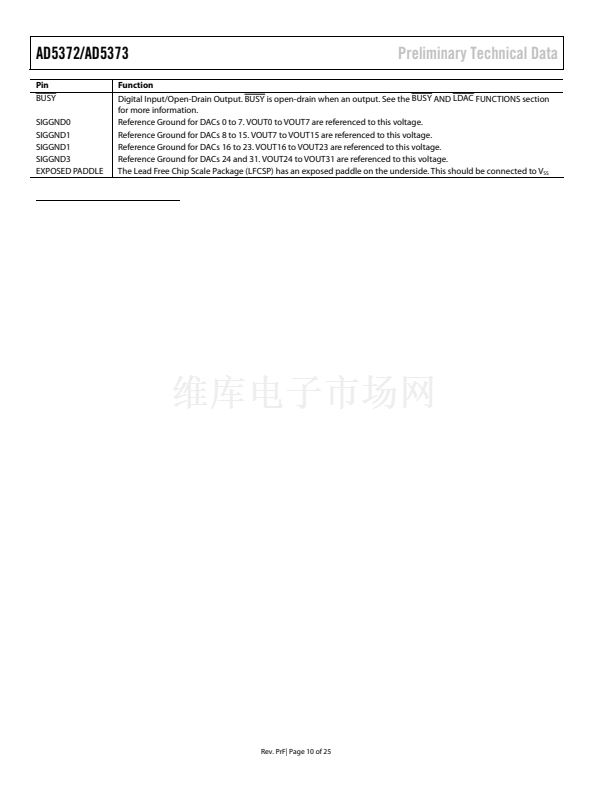
AD5372/AD5373
TIMING CHARACTERISTICS
Preliminary Technical Data
DV
CC
= 2.3 V to 5.5 V; V
DD
= 8 V to 16.5 V; V
SS
= 鈭?.5 V to 鈭?6.5 V; V
REF
= 3 V; AGND = DGND = SIGGND = 0 V;
R
L
= Open Circuit; Gain (m), Offset(c) and DAC Offset registers at default value; all specifications T
MIN
to T
MAX
, unless otherwise noted.
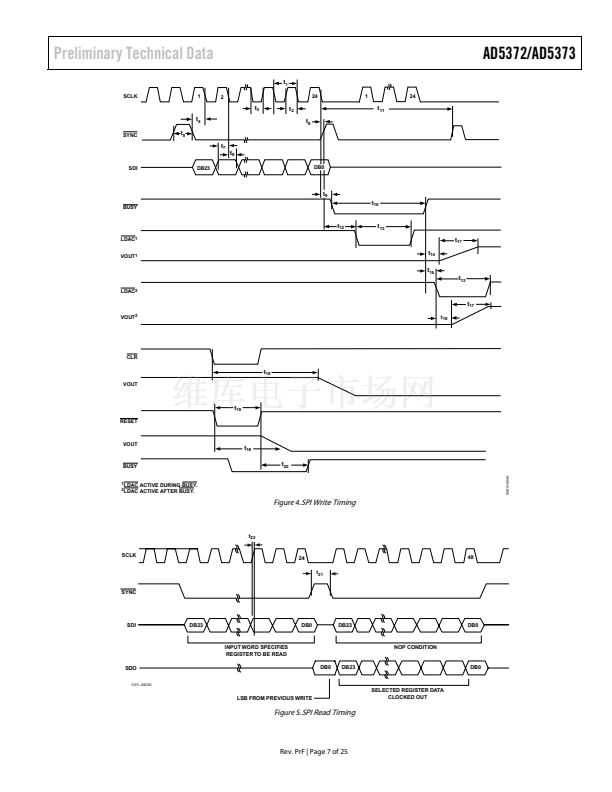
SPI INTERFACE (Figure
4 and Figure 5)
Parameter
1, 2, 3
t
1
t
2
t
3
t
4
t
5
t
6
t
7
t
8
t
93
t
10
t
11
t
12
t
13
t
14
t
15
t
16
t
17
t
18
t
19
t
20
t
21
t
225
1
2
Limit at T
MIN
, T
MAX
20
8
8
11
20
10
5
5
42
1.25
500
20
10
3
0
3
20/30
125
330
400
270
25
Unit
ns min
ns min
ns min
ns min
ns min
ns min
ns min
ns min
ns max
碌s max
ns max
ns min
ns min
Description
SCLK Cycle Time.
SCLK High Time.
SCLK Low Time.
SYNC Falling Edge to SCLK Falling Edge Setup Time.
Minimum SYNC High Time.
24th SCLK Falling Edge to SYNC Rising Edge.
Data Setup Time.
Data Hold Time.
SYNC Rising Edge to BUSY Falling Edge.
BUSY
Pulse Width Low (Single-Channel Update.) See
Table 7.
Single-Channel Update Cycle Time
24th SCLK Falling Edge to LDAC Falling Edge.
LDAC Pulse Width Low.
BUSY Rising Edge to DAC Output Response Time.
BUSY Rising Edge to LDAC Falling Edge.
LDAC Falling Edge to DAC Output Response Time.
DAC Output Settling Time.
CLR/RESET Pulse Activation Time.
RESET Pulse Width Low.
RESET Time Indicated by BUSY
Low.
Minimum SYNC High Time in Readback Mode.
SCLK Rising Edge to SDO Valid.
碌s max
ns min
碌s max
碌s typ/max
ns max
ns min
碌s max
ns min
ns max
Guaranteed by design and characterization, not production tested.
All input signals are specified with t
r
= t
f
= 2 ns (10% to 90% of V
CC
) and timed from a voltage level of 1.2 V.
3
See Figure 4 and Figure 5.
4
This is measured with the load circuit of Figure 2.
5
This is measured with the load circuit of Figure 3.
V
CC
200碌A(chǔ)
I
OL
R
L
TO
OUTPUT
PIN
2.2k鈩?/div>
TO
OUTPUT
PIN
C
L
50pF
200碌A(chǔ)
I
OL
V
OH
(min) - V
OL
(max)
2
V
OL
C
L
50pF
Figure 2. Load Circuit for BUSY Timing Diagram
Figure 3. Load Circuit for SDO Timing Diagram
Rev. PrF| Page 6 of 25


 1
1
 2
2
 3
3
 4
4
 5
5
 6
6
 7
7
 8
8
 9
9
 10
10
 11
11
 12
12
 13
13
 14
14
 15
15
 16
16
 17
17
 18
18
 19
19
 20
20
 21
21
 22
22
 23
23
 24
24
 25
25
