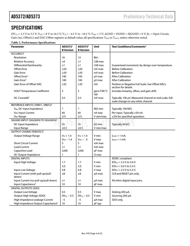
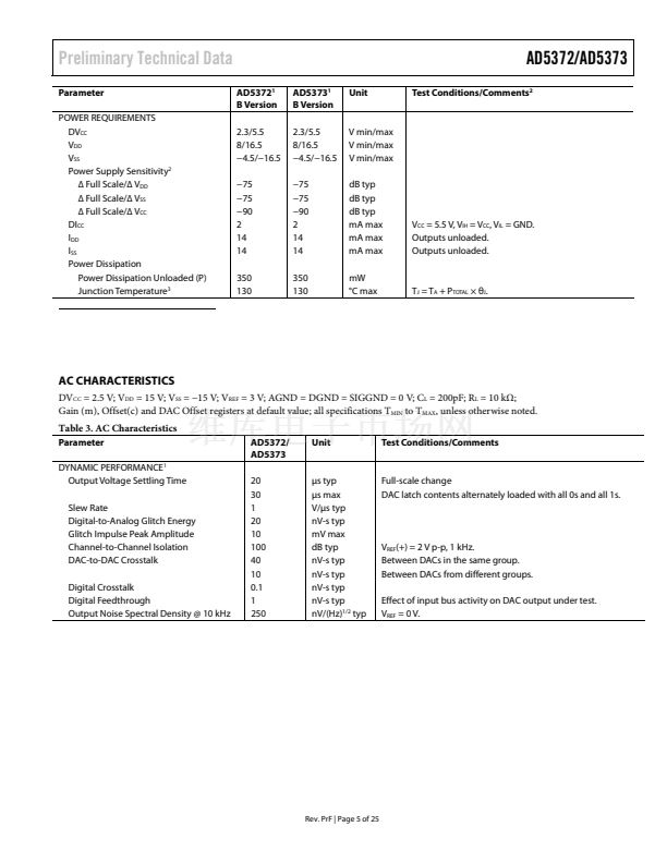
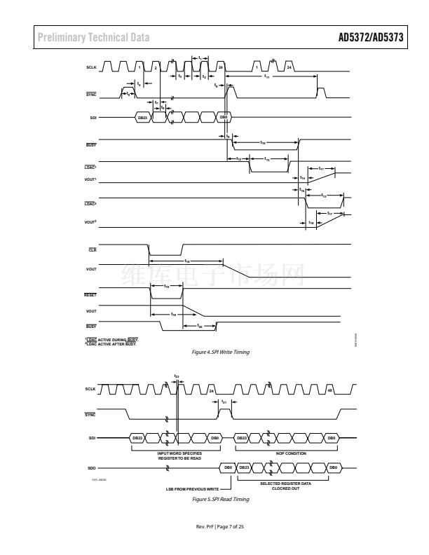
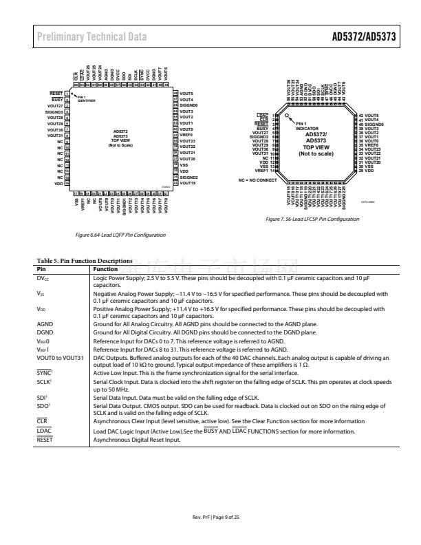
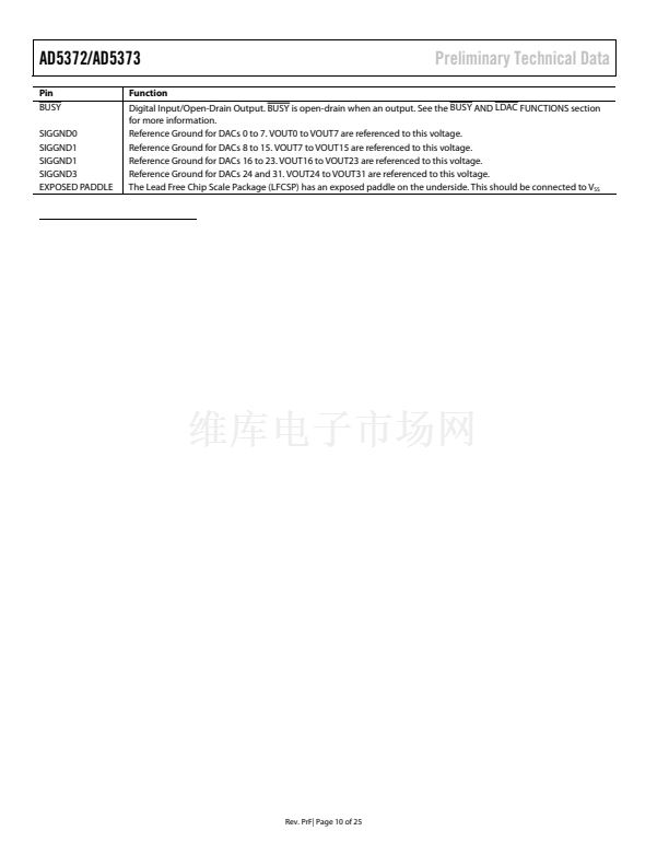
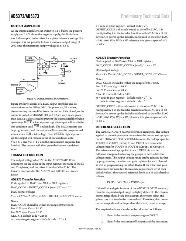
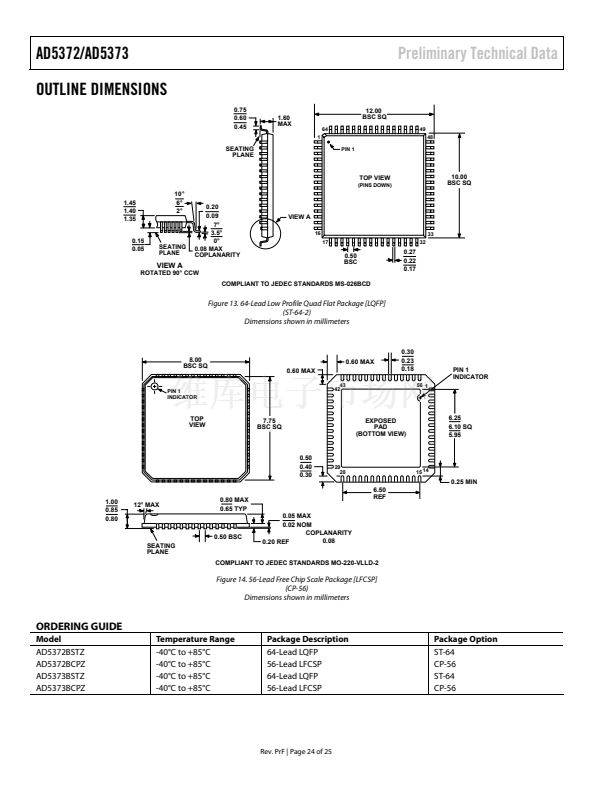
AD5372/AD5373
Table 17. DACs Select by A/B Select Registers
A/B Select
Register
0
1
2
3
Bits
F7
VOUT7
VOUT15
VOU23
VOUT31
F6
VOUT6
VOUT14
VOUT22
VOUT30
F5
VOUT5
VOUT13
VOUT21
VOUT29
F4
VOUT4
VOUT12
VOUT20
VOUT28
F3
VOUT3
VOUT11
VOUT19
VOUT27
F2
VOUT2
Preliminary Technical Data
F1
VOUT1
VOUT9
VOUT17
VOUT25
F0
VOUT0
VOUT8
VOUT16
VOUT24
VOUT10
VOUT18
VOUT26
POWER SUPPLY DECOUPLING
In any circuit where accuracy is important, careful considera-
tion of the power supply and ground return layout helps to
ensure the rated performance. The printed circuit board on
which the AD5372/AD5373 is mounted should be designed so
that the analog and digital sections are separated and confined
to certain areas of the board. If the AD5372/AD5373 is in a
system where multiple devices require an AGND-to-DGND
connection, the connection should be made at one point only.
The star ground point should be established as close as possible
to the device. For supplies with multiple pins (V
SS
, V
DD
, V
CC
), it
is recommended to tie these pins together and to decouple each
supply once.
The AD5372/AD5373 should have ample supply decoupling of
10 碌F in parallel with 0.1 碌F on each supply located as close to
the package as possible, ideally right up against the device. The
10 碌F capacitors are the tantalum bead type. The 0.1 碌F capaci-
tor should have low effective series resistance (ESR) and
effective series inductance (ESI), such as the common ceramic
types that provide a low impedance path to ground at high
frequencies, to handle transient currents due to internal logic
switching.
Digital lines running under the device should be avoided,
because these couple noise onto the device. The analog ground
plane should be allowed to run under the AD5372/AD5373 to
avoid noise coupling. The power supply lines of the
AD5372/AD5373 should use as large a trace as possible to
provide low impedance paths and reduce the effects of glitches
on the power supply line. Fast switching digital signals should
be shielded with digital ground to avoid radiating noise to other
parts of the board, and should never be run near the reference
inputs. It is essential to mini mize noise on all V
REF
lines.
Avoid crossover of digital and analog signals. Traces on
opposite sides of the board should run at right angles to each
other. This reduces the effects of feedthrough through the
board. A microstrip technique is by far the best, but not always
possible with a double-sided board. In this technique, the
component side of the board is dedicated to ground plane,
while signal traces are placed on the solder side.
As is the case for all thin packages, care must be taken to avoid
flexing the package and to avoid a point load on the surface of
this package during the assembly process.
POWER SUPPLY SEQUENCING
When the supplies are connected to the AD5372/AD5373 it is
important that the AGND and DGND pins are connected to the
relevant ground plane before the positive or negative supplies
are applied. In most applications this is not an issue as the
ground pins for the power supplies will be connected to the
ground pins of the AD5372/AD5373 via ground planes. Where
the AD5372/AD5373 is to be used in a hot-swap card care
should be taken to ensure that the ground pins are connected to
the supply grounds before the positive or negative supplies are
connected. This is required to prevent currents flowing in
directions other than towards an analog or digital ground.
Rev. PrF | Page 22 of 25


 1
1
 2
2
 3
3
 4
4
 5
5
 6
6
 7
7
 8
8
 9
9
 10
10
 11
11
 12
12
 13
13
 14
14
 15
15
 16
16
 17
17
 18
18
 19
19
 20
20
 21
21
 22
22
 23
23
 24
24
 25
25
