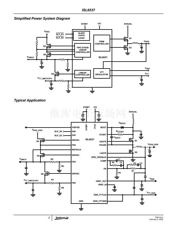
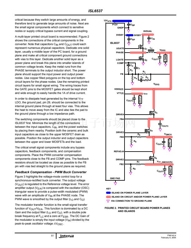
ISL6537
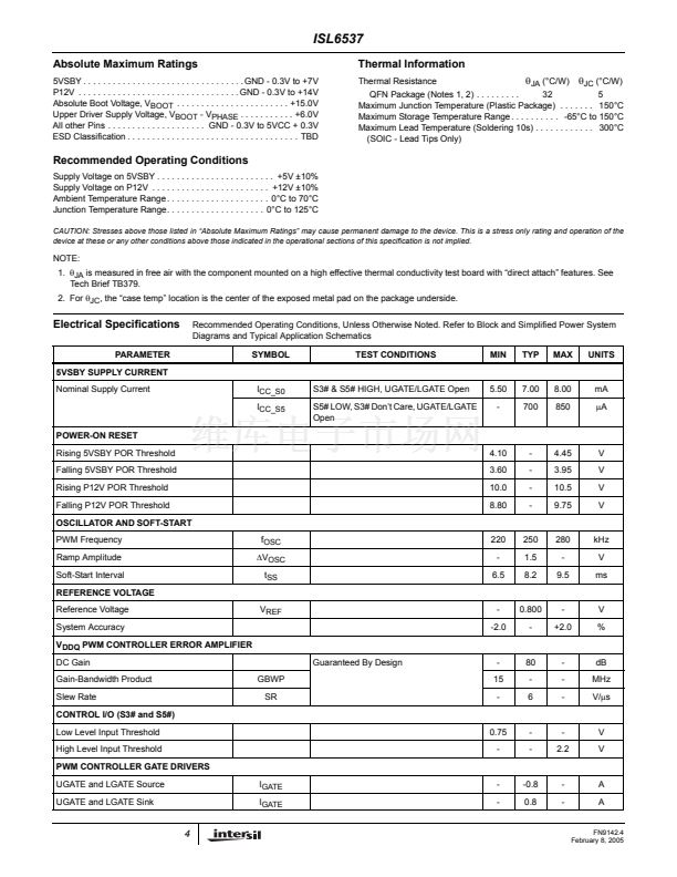
BOOT (Pin 25)
This pin provides ground referenced bias voltage to the
upper MOSFET driver. A bootstrap circuit is used to create a
voltage suitable to drive a logic-level N-channel MOSFET.
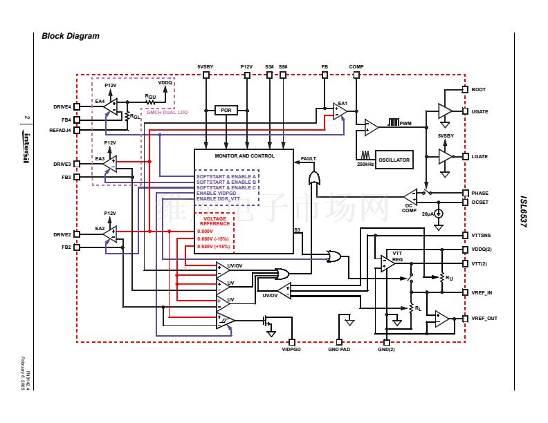
Functional Description
Overview
The ISL6537 provides complete control, drive, protection
and ACPI compliance for a regulator powering DDR memory
systems and the GMCH core and GMCH/CPU termination
rails. It is primarily designed for computer applications
powered from an ATX power supply.
A 250kHz Synchronous Buck Regulator with a precision
0.8V reference provides the proper Core voltage to the
system memory of the computer. An internal LDO regulator
with the ability to both sink and source current and an
externally available buffered reference that tracks the V
DDQ
output by 50% provides the V
TT
termination voltage.
A dual stage LDO controller provides the GMCH core
voltage. A third LDO controller is included for the regulation
of the GMCH/CPU termination rail.
ACPI compliance is realized through the SLP_S3 and
SLP_S5 sleep signals and through monitoring of the 12V
ATX bus.
FB2 (Pin 11)
Connect the output of the V
TT_GMCH/CPU
linear regulator to
this pin through a properly sized resistor divider. The voltage
at this pin is regulated to 0.8V. This pin is monitored for
under-voltage events.
DRIVE2 (Pin 10)
This pin provides the gate voltage for the V
TT_GMCH/CPU
linear regulator pass transistor. Connect this pin to the gate
terminal of an external N-Channel MOSFET transistor.
FB3 (Pin 18)
Connect the output of the lower V
GMCH
linear regulator to
this pin through a properly sized resistor divider. The voltage
at this pin is regulated to 0.8V. This pin is monitored for
under-voltage events.
DRIVE3 (Pin 19)
This pin provides the gate voltage for the lower V
GMCH
linear regulator pass transistor. Connect this pin to the gate
terminal of an external N-Channel MOSFET transistor.
Initialization
The ISL6537 automatically initializes upon receipt of input
power. Special sequencing of the input supplies is not
necessary. The Power-On Reset (POR) function continually
monitors the input bias supply voltages. The POR monitors
the bias voltage at the 5VSBY and P12V pins. The POR
function initiates soft-start operation after the bias supply
voltages exceed their POR thresholds.
FB4 (Pin 20)
Connect the output of the upper V
GMCH
linear regulator to
this pin. The voltage at this pin is regulated via the RAFADJ4
pin.
DRIVE4 (Pin 21)
This pin provides the gate voltage for the upper V
GMCH
linear regulator pass transistor. Connect this pin to the gate
terminal of an external N-Channel MOSFET transistor.
ACPI State Transitions
Figure 1 shows how the individual regulators are controlled
during all state transitions. All references to timing in this
section are in reference to Figure 1.
Cold Start (S4/S5 to S0 Transition)
At the onset of a mechanical start, time t
0
in Figure 1, the
ISL6537 receives its bias voltage from the 5V Standby bus
(5VSBY). Once the 5VSBY rail has exceeded the POR
threshold, the ISL6537 will remain in an internal S5 state
until both the SLP_S3 and SLP_S5 signal have transitioned
high and the 12V POR threshold has been exceeded by the
+12V rail from the ATX, which occurs at time t
1
.
Once all of these conditions are met, the PWM error
amplifier will first be reset by internally shorting the COMP
pin to the FB pin. This reset lasts for three soft start cycles,
which is typically 24ms (one soft start cycle is typically
8.2ms). The digital soft start sequence will then begin. Each
regulator is enabled and soft-started according to a preset
sequence.
At time t
2
, the 3 soft-start cycle reset has ended and the
V
DDQ_DDR
rail and the upper V
GMCH
LDO are digitally soft-
started.
REFADJ4 (Pin 20)
This pin controls the reference for the upper V
GMCH
linear
regulator. To insure that both upper and lower pass
transistors dissipate the same power, tie this pin to the
V
GMCH
output rail.
VIDPGD (Pin 12)
The VIDPGD pin is an open-drain logic output that changes
to a logic low if the V
TT_GMCH/CPU
linear regulator is out of
regulation in S0/S1/S2 state. VIDPGD will always be low in
any state other than S0/S1/S2.
S5# (Pin 23)
This pin accepts the SLP_S5# sleep state signal.
S3# (Pin 2)
This pin accepts the SLP_S3# sleep state signal.
7
FN9142.4
February 8, 2005


 1
1
 2
2
 3
3
 4
4
 5
5
 6
6
 7
7
 8
8
 9
9
 10
10
 11
11
 12
12
 13
13
 14
14
 15
15
