廬
ISL6537
Data Sheet
February 8, 2005
FN9142.4
ACPI Regulator/Controller for
Dual Channel DDR Memory Systems
The ISL6537 provides a complete ACPI compliant power
solution for up to 4 DIMM dual channel DDR/DDR2 Memory
systems. Included are both a synchronous buck controller to
supply V
DDQ
during S0/S1 and S3 states. During S0/S1
state, a fully integrated sink-source regulator generates an
accurate (V
DDQ
/2) high current V
TT
voltage without the
need for a negative supply. A buffered version of the V
DDQ
/2
reference is provided as V
REF
. Two LDO controllers are also
integrated for the GMCH core voltage regulation and for the
GMCH and CPU V
TT
termination voltage regulation.
The switching PWM controller drives two N-Channel
MOSFETs in a synchronous-rectified buck converter
topology. The synchronous buck converter uses voltage-
mode control with fast transient response. The switching
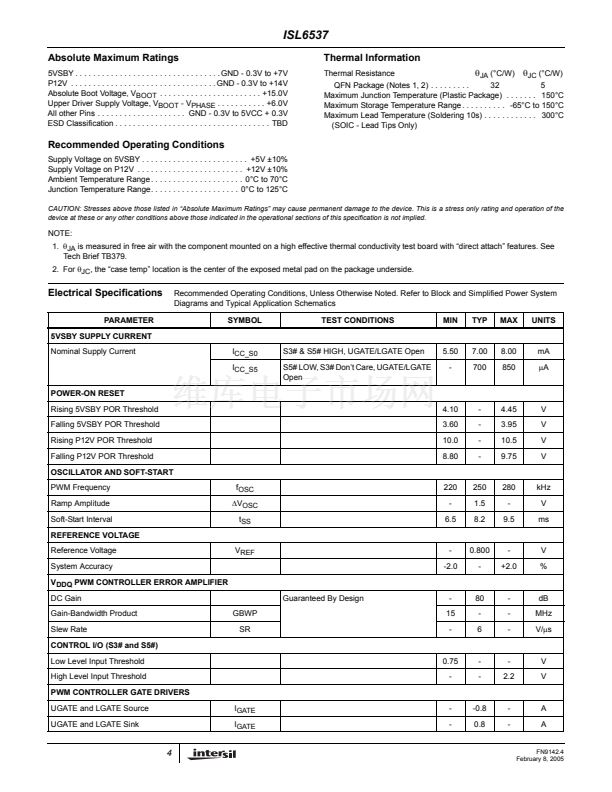
regulator provides a maximum static regulation tolerance of
鹵
2% over line, load, and temperature ranges. The output is
user-adjustable by means of external resistors down to 0.8V.
An integrated soft-start feature brings all outputs into
regulation in a controlled manner when returning to S0/S1
state from any sleep state. During S0 the VIDPGD signal
indicates that the GMCH and CPU V
TT
termination voltage
is within spec and operational.
Each output is monitored for undervoltage events. The
switching regulator also has overvoltage and over current
protection. Thermal shutdown is integrated.
Features
鈥?Generates 4 Regulated Voltages
- Synchronous Buck PWM Controller for DDR V
DDQ
- 3A Integrated Sink/Source Linear Regulator with
Accurate VDDQ/2 Divider Reference for DDR V
TT
- LDO Regulator for GMCH Core
- LDO Regulator for CPU/GMCH V
TT
Termination
鈥?ACPI compliant sleep state control
鈥?Glitch-free Transitions During State Changes
鈥?Integrated V
REF
Buffer
鈥?PWM Controller Drives Low Cost N-Channel MOSFETs
鈥?250kHz Constant Frequency Operation
鈥?Tight Output Voltage Regulation
- All Outputs:
鹵
2% Over Temperature
鈥?Fully-Adjustable Outputs with Wide Voltage Range: Down
to 0.8V supports DDR and DDR2 Specifications
鈥?Simple Single-Loop Voltage-Mode PWM Control Design
鈥?Fast PWM Converter Transient Response
鈥?Under and Over-voltage Monitoring on All Outputs
鈥?OCP on the Switching Regulator
鈥?Integrated Thermal Shutdown Protection
鈥?Pb-Free Available (RoHS Compliant)
Applications
鈥?Single and Dual Channel DDR Memory Power Systems in
ACPI compliant PCs
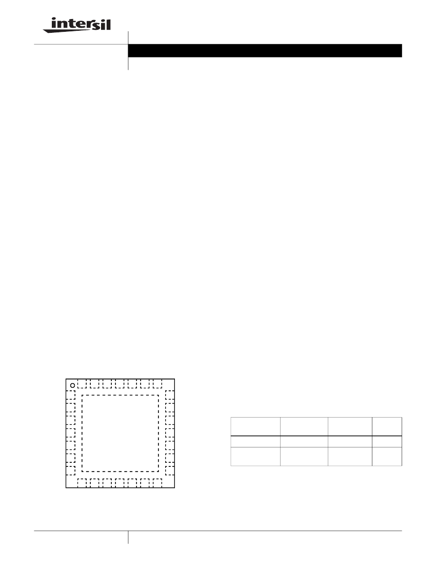
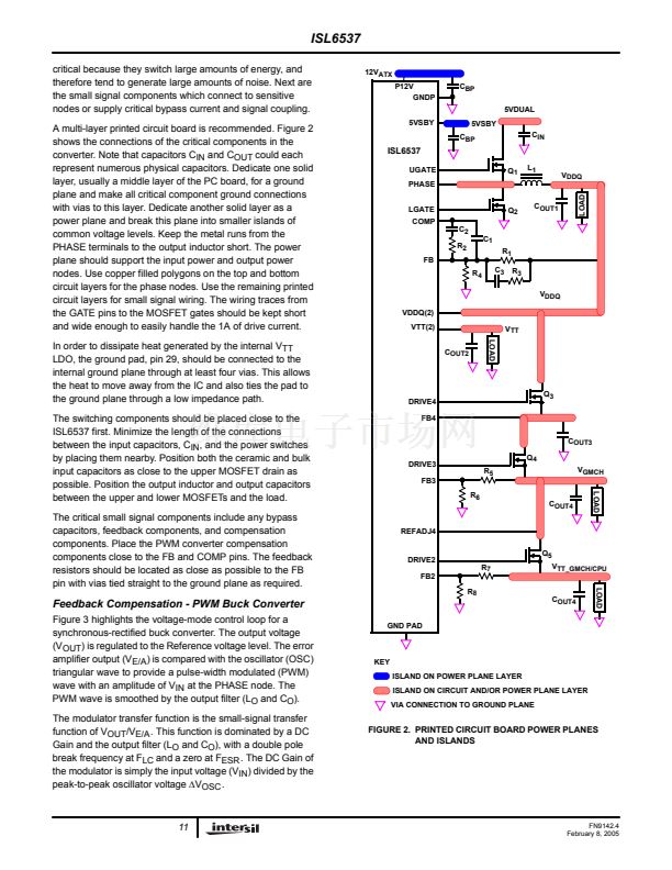
Pinout
LGATE
ISL6537 (6x6 QFN)
TOP VIEW
OCSET
PHASE
UGATE
BOOT
GND
S5#
鈥?Graphics cards - GPU and memory supplies
鈥?ASIC power supplies
鈥?Embedded processor and I/O supplies
21 DRIVE4
20 REFADJ4
19 DRIVE3
28
5VSBY
S3#
P12V
GND
DDR_VTT
DDR_VTT
VDDQ
1
2
3
4
5
6
7
8
VDDQ
27
26
25
24
23
22
鈥?DSP supplies
Ordering Information
PART NUMBER
ISL6537CR
ISL6537CRZ
(See Note)
TEMP. RANGE
(擄C)
0 to 70
0 to 70
PACKAGE
PKG.
DWG. #
GND
29
18 FB3
17 FB4
16 COMP
15 FB
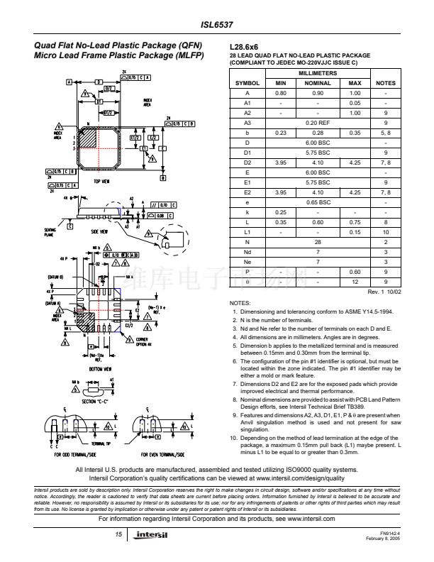
28 Ld 6x6 QFN L28.6x6
28 Ld 6x6 QFN L28.6x6
(Pb-free)
*Add 鈥?T鈥?suffix to part number for tape and reel packaging.
NOTE: Intersil Pb-free products employ special Pb-free material
sets; molding compounds/die attach materials and 100% matte tin
plate termination finish, which are RoHS compliant and compatible
with both SnPb and Pb-free soldering operations. Intersil Pb-free
products are MSL classified at Pb-free peak reflow temperatures that
meet or exceed the Pb-free requirements of IPC/JEDEC J STD-020.
CAUTION: These devices are sensitive to electrostatic discharge; follow proper IC Handling Procedures.
1-888-INTERSIL or 321-724-7143
|
Intersil (and design) is a registered trademark of Intersil Americas Inc.
Copyright 漏 Intersil Americas Inc. 2004, 2005. All Rights Reserved
All other trademarks mentioned are the property of their respective owners.
9
DDR_VTTSNS
10
DRIVE2
11
FB2
12
VIDPGD
13
VREF_OUT
14
VREF_IN
1


 1
1
 2
2
 3
3
 4
4
 5
5
 6
6
 7
7
 8
8
 9
9
 10
10
 11
11
 12
12
 13
13
 14
14
 15
15
