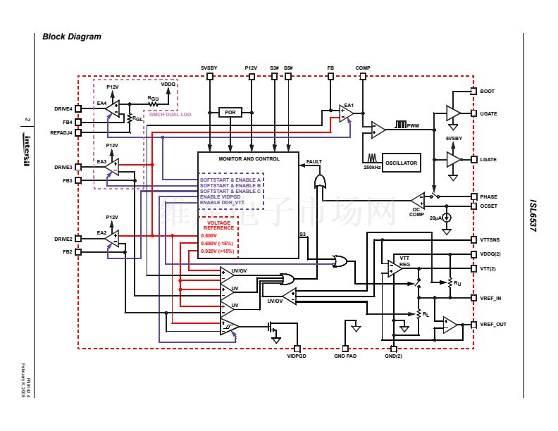
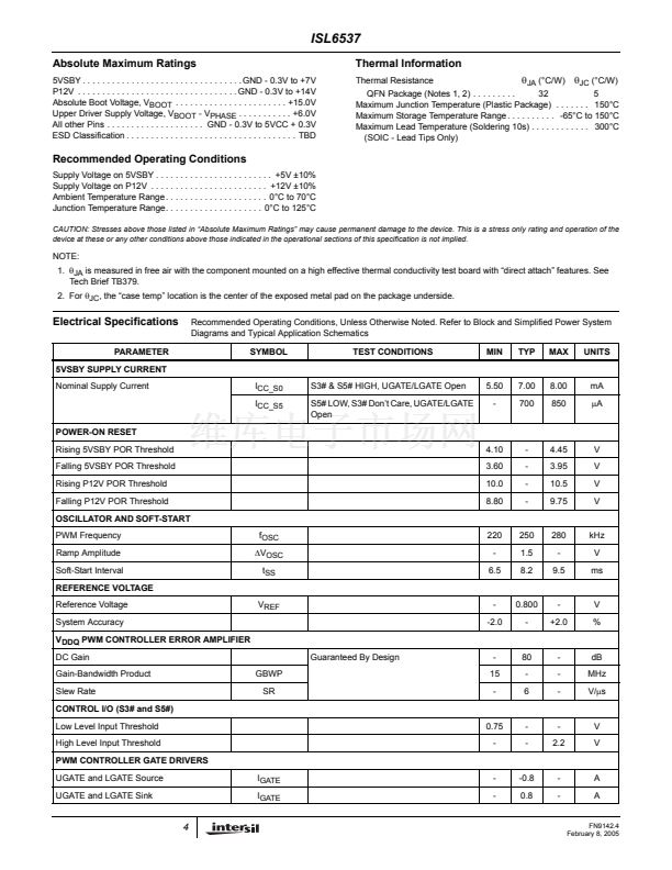
ISL6537
Functional Pin Description
5VSBY (Pin 1)
5VSBY is the bias supply of the ISL6537. It is typically
connected to the 5V standby rail of an ATX power supply.
During S4/S5 sleep states the ISL6537 enters a reduced
power mode and draws less than 1mA (I
CC_S5
) from the
5VSBY supply. The supply to 5VSBY should be locally
bypassed using a 0.1碌F capacitor.
PHASE
(Pin 24)
Connect this pin to the upper MOSFET鈥檚 source. This pin is
used to monitor the voltage drop across the upper MOSFET
for over-current protection.
OCSET
(Pin 22)
Connect a resistor (R
OCSET
) from this pin to the drain of the
upper MOSFET. R
OCSET
, an internal 20碌A(chǔ) current source
(I
OCSET
), and the upper MOSFET on-resistance (r
DS(ON)
)
set the converter over-current (OC) trip point according to
the following equation:
I
OCSET
xR
OCSET
I
PEAK
= -------------------------------------------------
r
DS
(
ON
)
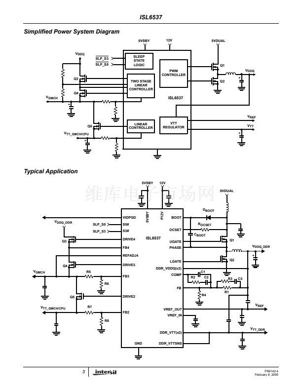
P12V (Pin 3)
The V
TT
regulation circuit and the Linear Drivers are
powered by P12V. P12V is not required during S3/S4/S5
operation. P12V is typically connected to the +12V rail of an
ATX power supply.
GND (Pins 4, 27, 29)
The GND terminals of the ISL6537 provide the return path
for the V
TT
LDO, and switching MOSFET gate drivers. High
ground currents are conducted directly through the exposed
paddle of the QFN package which must be electrically
connected to the ground plane through a path as low in
inductance as possible.
An over-current trip cycles the soft-start function.
VDDQ (Pins 7, 8)
The VDDQ pins should be connected externally together to
the regulated V
DDQ
output. During S0/S1 states, the VDDQ
pins serve as inputs to the V
TT
regulator and to the V
TT
Reference precision divider.
UGATE (Pin 26)
Connect this pin to the upper MOSFET鈥檚 gate. This pin
provides the PWM-controlled gate drive for the upper
MOSFET. This pin is also monitored by the adaptive shoot-
through protection circuitry to determine when the upper
MOSFET has turned off. Do not insert any circuitry between
this pin and the gate of the upper MOSFET, as it may
interfere with the internal adaptive shoot-through protection
circuitry and render it ineffective.
DDR_VTT (Pins 5, 6)
The DDR_VTT pins should be connect externally together.
During S0/S1 states, the DDR_VTT pins serve as the
outputs of the V
TT
linear regulator. During S3 state, the V
TT
regulator is disabled.
DDR_VTTSNS (Pin 9)
VTTSNS is used as the feedback for control of the V
TT
linear
regulator. Connect this pin to the V
TT
output at the physical
point of desired regulation.
LGATE (Pin 28)
Connect this pin to the lower MOSFET鈥檚 gate. This pin
provides the PWM-controlled gate drive for the lower
MOSFET. This pin is also monitored by the adaptive shoot-
through protection circuitry to determine when the lower
MOSFET has turned off. Do not insert any circuitry between
this pin and the gate of the lower MOSFET, as it may
interfere with the internal adaptive shoot-through protection
circuitry and render it ineffective.
VREF_OUT (Pin 13)
VREF_OUT is a buffered version of V
TT
and also acts as the
reference voltage for the V
TT
linear regulator. It is
recommended that a minimum capacitance of 0.1碌F is
connected between V
DDQ
and VREF_OUT and also
between VREF_OUT and ground for proper operation.
VREF_IN (Pin 14)
A capacitor, C
SS
, connected between VREF_IN and ground
is required. This capacitor and the parallel combination of
the Upper and Lower Divider Impedance (R
U
||R
L
), sets the
time constant for the start up ramp when transitioning from
S3/S4/S5 to S0/S1/S2.
The minimum value for C
SS
can be found through the
following equation:
C
VTTOUT
鈰?/div>
V
DDQ
C
SS
>
------------------------------------------------
10
鈰?/div>
2A
鈰?/div>
R
U
||
R
L
FB (Pin 15) and COMP (Pin 16)
The V
DDQ
switching regulator employs a single voltage
control loop. FB is the negative input to the voltage loop error
amplifier. The V
DDQ
output voltage is set by an external
resistor divider connected to FB. With a properly selected
divider, V
DDQ
can be set to any voltage between the power
rail (reduced by converter losses) and the 0.8V reference.
Loop compensation is achieved by connecting an AC
network across COMP and FB.
The FB pin is also monitored for under and over-voltage
events.
The calculated capacitance, C
SS
, will charge the output
capacitor bank on the V
TT
rail in a controlled manner without
reaching the current limit of the V
TT
LDO.
6
FN9142.4
February 8, 2005


 1
1
 2
2
 3
3
 4
4
 5
5
 6
6
 7
7
 8
8
 9
9
 10
10
 11
11
 12
12
 13
13
 14
14
 15
15
