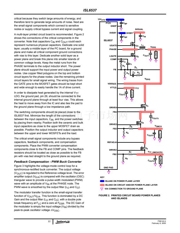
k鈩?/div>
mA
A
Recommended Operating Conditions, Unless Otherwise Noted. Refer to Block and Simplified Power System
Diagrams and Typical Application Schematics
(Continued)
SYMBOL
TEST CONDITIONS
MIN
TYP
MAX
UNITS
LINEAR REGULATORS
DC GAIN
Gain Bandwidth Product
Slew Rate
DRIVEn High Output Voltage
DRIVEn Low Output Voltage
DRIVEn High Output Source Current
DRIVEn Low Output Sink Current
VIDPGD
V
TT_GMCH/CPU
Rising Threshold
V
TT_GMCH/CPU
Falling Threshold
PROTECTION
OCSET Current Source
V
TT_DDR
Current Limit
V
DDQ
OV Level
V
DDQ
UV Level
V
TT_DDR
OV Level
V
TT_DDR
UV Level
V
GMCH
UV Level
V
TT_GMCH/CPU
UV Level
Thermal Shutdown Limit
V
FB
/V
REF
V
FB
/V
REF
V
TT
/V
VREF_IN
V
TT
/V
VREF_IN
V
FB4
/V
REF
V
FB2
/V
REF
T
SD
I
OCSET
By Design
S0/S3
S0/S3
S0
S0
S0
S0
By Design
18
-3.3
-
-
-
-
-
-
-
20
-
115
75
115
85
75
75
140
22
3.3
-
-
-
-
-
-
-
碌A(chǔ)
A
%
%
%
%
%
%
擄C
S0
S0
0.725
-
0.74
0.70
-
0.715
V
V
V
FB
= 770mV; V
DRIVEn
= 0V
V
FB
= 830mV; V
DRIVEn
= 10V
GBWP
SR
DRIVEn unloaded
Guaranteed By Design
-
15
-
9.75
-
-
-
80
-
6
10.0
0.16
1.7
1.2
-
-
-
-
0.50
2.6
1.75
dB
MHz
V/碌s
V
V
mA
mA
5
FN9142.4
February 8, 2005


 1
1
 2
2
 3
3
 4
4
 5
5
 6
6
 7
7
 8
8
 9
9
 10
10
 11
11
 12
12
 13
13
 14
14
 15
15
