錚?/div>
FIGURE 3. VOLTAGE-MODE BUCK CONVERTER
COMPENSATION DESIGN AND OUTPUT
VOLTAGE SELECTION
100
80
F
Z1
F
Z2
F
P1
F
P2
OPEN LOOP
ERROR AMP GAIN
Modulator Break Frequency Equations
GAIN (dB)
60
40
20
0
-20
-40
-60
10
100
1K
MODULATOR
GAIN
F
LC
10K
F
ESR
100K
20LOG
(R
2
/R
1
)
1
-
F LC
= ------------------------------------------
2蟺
x
L O
x
C O
1
-
F ESR
= -------------------------------------------
2蟺
x
ESR
x
C O
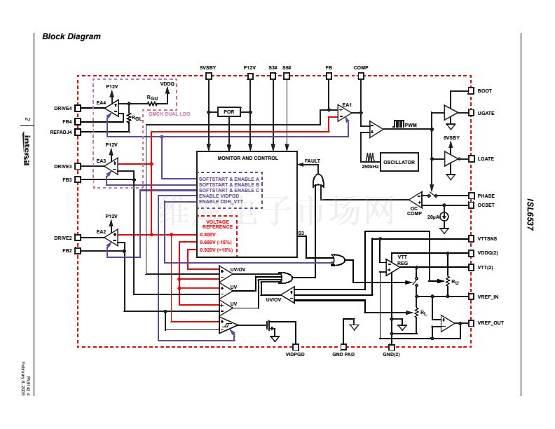
The compensation network consists of the error amplifier
(internal to the ISL6537) and the impedance networks Z
IN
and Z
FB
. The goal of the compensation network is to provide
a closed loop transfer function with the highest 0dB crossing
frequency (f
0dB
) and adequate phase margin. Phase margin
is the difference between the closed loop phase at f
0dB
and
180 degrees. The equations below relate the compensation
network鈥檚 poles, zeros and gain to the components (R
1
, R
2
,
R
3
, C
1
, C
2
, and C
3
) in Figure 5. Use these guidelines for
locating the poles and zeros of the compensation network:
1. Pick Gain (R
2
/R
1
) for desired converter bandwidth.
2. Place 1
ST
Zero Below Filter鈥檚 Double Pole (~75% F
LC
).
3. Place 2
ND
Zero at Filter鈥檚 Double Pole.
4. Place 1
ST
Pole at the ESR Zero.
5. Place 2
ND
Pole at Half the Switching Frequency.
6. Check Gain against Error Amplifier鈥檚 Open-Loop Gain.
7. Estimate Phase Margin - Repeat if Necessary.
20LOG
(V
IN
/鈭哣
OSC
)
COMPENSATION
GAIN
CLOSED LOOP
GAIN
1M
10M
FREQUENCY (Hz)
FIGURE 4. ASYMPTOTIC BODE PLOT OF CONVERTER GAIN
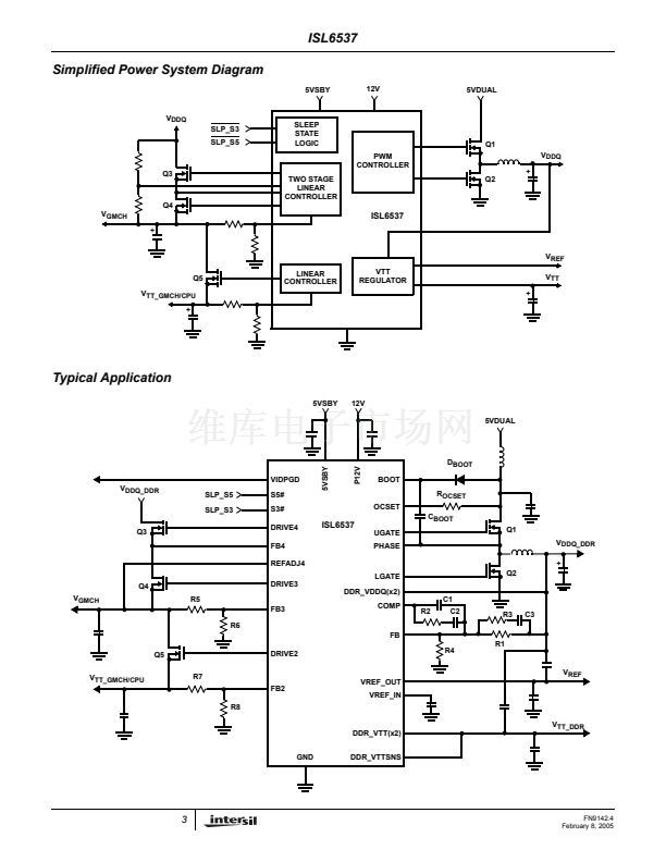
Output Voltage Selection
The output voltage of the all the external voltage regulators
converter can be programmed to any level between their
individual input voltage and the internal reference, 0.8V. An
external resistor divider is used to scale the output voltage
relative to the reference voltage and feed it back to the
inverting input of the error amplifier, refer to the Typical
Application on page 3.
12
FN9142.4
February 8, 2005


 1
1
 2
2
 3
3
 4
4
 5
5
 6
6
 7
7
 8
8
 9
9
 10
10
 11
11
 12
12
 13
13
 14
14
 15
15
