2.4 GHz High-Linearity Power Amplifier
SST12LP10
Preliminary Specifications
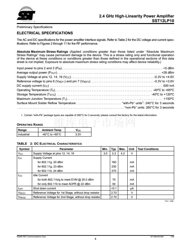
ELECTRICAL SPECIFICATIONS
The AC and DC specifications for the power amplifier interface signals. Refer to Table 2 for the DC voltage and current spec-
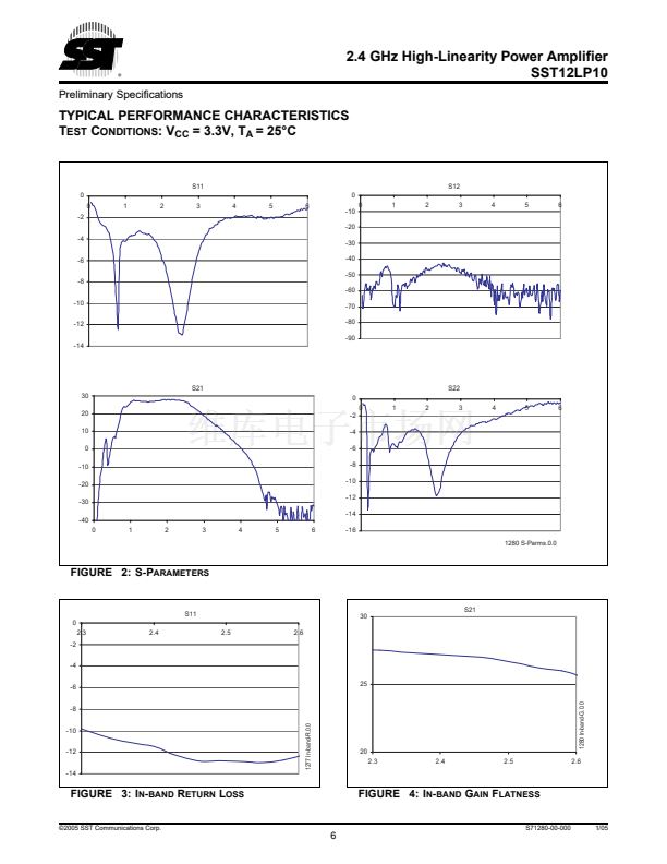
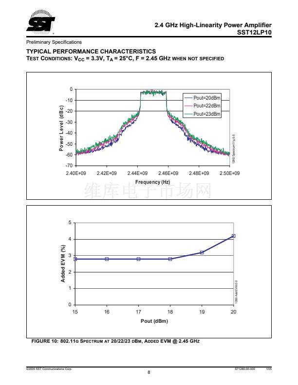
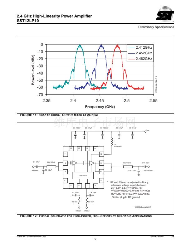
ifications. Refer to Figures 2 through 11 for the RF performance.
Absolute Maximum Stress Ratings
(Applied conditions greater than those listed under 鈥淎bsolute Maximum
Stress Ratings鈥?may cause permanent damage to the device. This is a stress rating only and functional operation
of the device at these conditions or conditions greater than those defined in the operational sections of this data
sheet is not implied. Exposure to absolute maximum stress rating conditions may affect device reliability.)
Input power to pins 2 and 3 (P
IN
) . . . . . . . . . . . . . . . . . . . . . . . . . . . . . . . . . . . . . . . . . . . . . . . . . . . . . . . . . . +5 dBm
Average output power (P
OUT
). . . . . . . . . . . . . . . . . . . . . . . . . . . . . . . . . . . . . . . . . . . . . . . . . . . . . . . . . . . . +28 dBm
Supply Voltage at pins 12, 14, 16 (V
CC
) . . . . . . . . . . . . . . . . . . . . . . . . . . . . . . . . . . . . . . . . . . . . . . . . -0.3V to +4.6V
Reference voltage to pins 6 (V
REF1
) and pin 7 (V
REF2
) . . . . . . . . . . . . . . . . . . . . . . . . . . . . . . . . . . . . -0.3V to +3.6V
DC supply current (I
CC
) . . . . . . . . . . . . . . . . . . . . . . . . . . . . . . . . . . . . . . . . . . . . . . . . . . . . . . . . . . . . . . . . . 500 mA
Operating Temperature (T
A
) . . . . . . . . . . . . . . . . . . . . . . . . . . . . . . . . . . . . . . . . . . . . . . . . . . . . . . . . -40潞C to +85潞C
Storage Temperature (T
STG
) . . . . . . . . . . . . . . . . . . . . . . . . . . . . . . . . . . . . . . . . . . . . . . . . . . . . . . -40潞C to +120潞C
Maximum Junction Temperature (T
J
) . . . . . . . . . . . . . . . . . . . . . . . . . . . . . . . . . . . . . . . . . . . . . . . . . . . . . . . +150潞C
Surface Mount Solder Reflow Temperature: . . . . . . . . . . . . . . . . . . . . . . . . . 鈥渨ith-Pb鈥?units
1
: 240擄C for 3 seconds
. . . . . . . . . . . . . . . . . . . . . . . . . . . . . . . . . . . . . . . . . . . . . . . . . . . . . . . . . . . . . . 鈥渘on-Pb鈥?units: 260擄C for 3 seconds
1. Certain 鈥渨ith-Pb鈥?package types are capable of 260擄C for 3 seconds; please consult the factory for the latest information.
O
PERATING
R
ANGE
Range
Industrial
Ambient Temp
-40擄C to +85擄C
V
CC
3.3V
TABLE 2: DC E
LECTRICAL
C
HARACTERISTICS
Symbol
V
CC
I
CC
Supply Current
for 802.11g, 20 dBm
for 802.11g, 23 dBm
for 802.11b, 24 dBm
I
CQ
Idle Current
for both 802.11b/g to meet EVM @ 20.5 dBm
for only 802.11b to meet ACPR @ 22 dBm
I
OFF
V
REG1
V
REG2
Shut down current
Reference Voltage for 1st Stage, without drop resistor
Reference Voltage for 2nd Stage, without drop resistor
70
50
<0.1
2.70
2.70
mA
mA
碌A(chǔ)
V
V
T2.0 1280
Parameter
Supply Voltage at pins 12, 14, 16
Min.
3.0
Typ
3.3
160
230
270
Max.
4.2
Unit
V
mA
mA
mA
Test Conditions
漏2005 SST Communications Corp.
S71280-00-000
1/05
4


 1
1
 2
2
 3
3
 4
4
 5
5
 6
6
 7
7
 8
8
 9
9
 10
10
 11
11
 12
12
