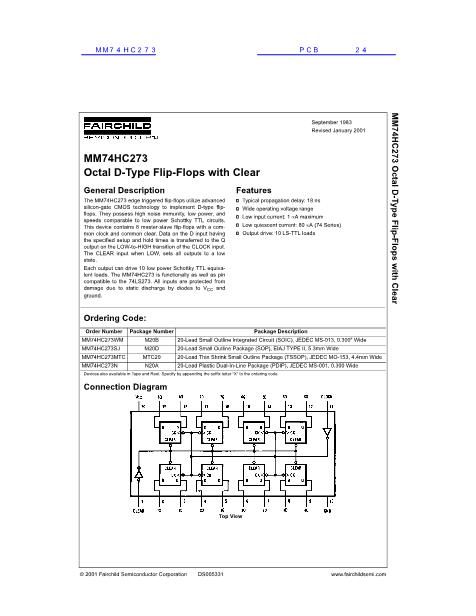
MM74HC273
Absolute Maximum Ratings
(Note 1)
(Note 2)
Supply Voltage (V
CC
)
DC Input Voltage (V
IN
)
DC Output Voltage (V
OUT
)
Clamp Diode Current (I
IK
, I
OK
)
DC Output Current, per pin (I
OUT
)
DC V
CC
or GND Current, per pin (I
CC
)
Storage Temperature Range (T
STG
)
Power Dissipation (P
D
)
(Note 3)
S.O. Package only
Lead Temperature (T
L
)
(Soldering 10 seconds)
260擄C
600 mW
500 mW
鈭?.5
to
+7.0V
鈭?.5
to V
CC
+1.5V
鈭?.5
to V
CC
+0.5V
鹵20
mA
鹵25
mA
鹵50
mA
鈭?5擄C
to
+150擄C
Recommended Operating
Conditions
Min
Supply Voltage (V
CC
)
DC Input or Output Voltage
(V
IN
, V
OUT
)
Operating Temperature Range (T
A
)
Input Rise or Fall Times
(t
r
, t
f
) V
CC
=
2.0V
V
CC
=
4.5V
V
CC
=
6.0V
1000
500
400
ns
ns
ns
0
鈭?0
V
CC
+85
V
擄C
2
Max
6
Units
V
Note 1:
Absolute Maximum Ratings are those values beyond which dam-
age to the device may occur.
Note 2:
Unless otherwise specified all voltages are referenced to ground.
Note 3:
Power Dissipation temperature derating 鈥?plastic 鈥淣鈥?package:
鈭?/div>
12 mW/擄C from 65擄C to 85擄C.
DC Electrical Characteristics
Symbol
V
IH
Parameter
Minimum HIGH Level
Input Voltage
V
IL
Maximum LOW Level
Input Voltage
V
OH
Minimum HIGH Level
Output Voltage
V
IN
=
V
IH
or V
IL
|I
OUT
|
鈮?/div>
20
碌A(chǔ)
Conditions
(Note 4)
V
CC
2.0V
4.5V
6.0V
2.0V
4.5V
6.0V
2.0V
4.5V
6.0V
2.0
4.5
6.0
4.2
5.7
0
0
0
0.2
0.2
T
A
=
25擄C
Typ
1.5
3.15
4.2
0.5
1.35
1.8
1.9
4.4
5.9
3.98
5.48
0.1
0.1
0.1
0.26
0.26
鹵0.1
8
T
A
= 鈭?0
to 85擄C T
A
= 鈭?5
to 125擄C
Guaranteed Limits
1.5
3.15
4.2
0.5
1.35
1.8
1.9
4.4
5.9
3.84
5.34
0.1
0.1
0.1
0.33
0.33
鹵1.0
80
1.5
3.15
4.2
0.5
1.35
1.8
1.9
4.4
5.9
3.7
5.2
0.1
0.1
0.1
0.4
0.4
鹵1.0
160
Units
V
V
V
V
V
V
V
V
V
V
V
V
V
V
V
V
碌A(chǔ)
碌A(chǔ)
V
IN
=
V
IH
or V
IL
|I
OUT
|
鈮?/div>
4.0 mA
|I
OUT
|
鈮?/div>
5.2 mA
V
OL
Maximum LOW Level
Output Voltage
V
IN
=
V
IH
or V
IL
|I
OUT
|
鈮?/div>
20
碌A(chǔ)
2.0V
4.5V
6.0V
V
IN
=
V
IH
or V
IL
|I
OUT
|
鈮?/div>
4 mA
|I
OUT
|
鈮?/div>
5.2 mA
I
IN
I
CC
Maximum Input
Current
Maximum Quiescent
Supply Current
V
IN
=
V
CC
or GND
I
OUT
=
0
碌A(chǔ)
6.0V
V
IN
=
V
CC
or GND
4.5V
6.0V
6.0V
4.5V
6.0V
Note 4:
For a power supply of 5V
鹵10%
the worst case output voltages (V
OH
, and V
OL
) occur for HC at 4.5V. Thus the 4.5V values should be used when
designing with this supply. Worst case V
IH
and V
IL
occur at V
CC
=
5.5V and 4.5V respectively. (The V
IH
value at 5.5V is 3.85V.) The worst case leakage cur-
rent (I
IN
, I
CC
, and I
OZ
) occur for CMOS at the higher voltage and so the 6.0V values should be used.
3
www.fairchildsemi.com
MM74HC273相關(guān)型號PDF文件下載
-
型號
版本
描述
廠商
下載
-
英文版
National Semiconductor [Synchronous Decade Counter with Asy...
NSC
-
英文版
Quad 2-Input NAND Gate, Quad 2-Input NOR Gate, Hex Inverter,...
NSC
-
英文版
Quad 2-Input NAND Gate . Quad 2-Input NOR Gate . Hex Inverte...
FAIRCHILD
-
英文版
Quad 2-Input NAND Gate . Quad 2-Input NOR Gate . Hex Inverte...
FAIRCHILD ...
-
英文版
Quad 2-Input NAND Gate, Quad 2-Input NOR Gate, Hex Inverter,...
NSC [Natio...
-
英文版
Quad 2-Input NAND Gate . Quad 2-Input NOR Gate . Hex Inverte...
FAIRCHILD
-
英文版
Quad 2-Input NAND Gate, Quad 2-Input NOR Gate, Hex Inverter,...
NSC
-
英文版
Quad 2-Input NAND Gate, Quad 2-Input NOR Gate, Hex Inverter,...
NSC [Natio...
-
英文版
Quad 2-Input NAND Gate . Quad 2-Input NOR Gate . Hex Inverte...
FAIRCHILD ...
-
英文版
Quad 2-Input NAND Gate . Quad 2-Input NOR Gate . Hex Inverte...
FAIRCHILD
-
英文版
Quad 2-Input NAND Gate, Quad 2-Input NOR Gate, Hex Inverter,...
NSC
-
英文版
Quad 2-Input NAND Gate, Quad 2-Input NOR Gate, Hex Inverter,...
NSC [Natio...
-
英文版
Quad 2-Input NAND Gate . Quad 2-Input NOR Gate . Hex Inverte...
FAIRCHILD ...
-
英文版
Quad 2-Input AND Gate
FAIRCHILD
-
英文版
Quad 2-Input AND Gate
NSC
-
英文版
Quad 2-Input AND Gate
NSC [Natio...
-
英文版
Quad 2-Input AND Gate
FAIRCHILD ...
-
英文版
Quad 2-Input NAND Gate, Quad 2-Input NOR Gate, Hex Inverter,...
NSC
-
英文版
Quad 2-Input NAND Gate, Quad 2-Input NOR Gate, Hex Inverter,...
NSC [Natio...
-
英文版
Hex Schmitt Trigger
NSC


 1
1
 2
2
 3
3
 4
4
 5
5
 6
6
 7
7
