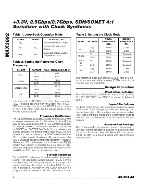
Table 1. Loop-Back Operation Mode
Table 3. Setting the Clock Mode
30k鈩?/div>
to
GND
GND
Table 2. Setting the Reference Clock
Frequency
CLKSET
V
CC
OPEN
30k鈩?to GND
GND
RATESET
V
CC
GND
V
CC
GND
V
CC
GND
V
CC
GND
RCLK鹵 FREQUENCY (MHz)
666
622
166.5
155.52
83.25
77.76
41.63
38.88
This reference clock can provide a clock hold-over sig-
nal to a clock and data recovery (CDR) circuit in the
event of loss of signal (LOS).
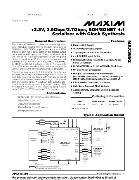
Design Procedure
Clock Mode Selection
The frequencies of the MAX3892 can be set up using
CLKSET, RATESET, and MODE as shown in Tables 2
and 3.
latching high FIFOERROR. To clear this condition,
RESET must be asserted high for at least 4UI. FIFOER-
ROR may be tied directly to the RESET input to recen-
ter the FIFO. After reset, the full elastic range of the
FIFO is available again.
Layout Techniques
For best performance, use good high-frequency layout
techniques. Filter voltage supplies and keep ground
connections short. Use multiple vias where possible.
Also, use controlled-impedance transmission lines to
interface with the MAX3892 clock and data inputs and
outputs.
Frequency Synthesizer
The PLL synthesizes a 2.5Gbps/2.7Gbps clock (SCLKO) from
an external reference clock. The PLL reference clock (RCLK)
may be 622.08MHz/666.53MHz, 155.52MHz/166.6MHz,
77.76MHz/83.3MHz or 38.88MHz/41.65MHz as determined
by CLKSET and RATESET. See Table 2 for the reference fre-
quency selection. The parallel output clock PCLKO is also
derived from the synthesizer to be SCLKO divided by 4. A
TTL-compatible loss-of-lock indicator,
LOL,
goes low when the
VCO is unable to lock to the reference frequency. Frequency
difference on RCLK with respect to the divided down SCLKO
greater than 500ppm is indicated by a low state on
LOL.
When the frequency difference between the clocks is less
than 250ppm,
LOL
high indicates a lock condition.
Exposed-Pad Package
The EP 44-pin QFN incorporates features that provide a
very low thermal-resistance path for heat removal from
the IC to a PC board. The MAX3892鈥檚 EP must be sol-
dered directly to a ground plane with good thermal
conductance.
System Loopback
The MAX3892 is designed to allow system loop-back
testing. The loop-back outputs (SLBO+, SLBO-) of the
MAX3892 may be directly connected to the loop-back
inputs of a deserializer (such as the MAX3882) for sys-
tem diagnostics. Alternatively, the SLBO pins can be
programmed to provide a 622MHz reference clock.
8
_______________________________________________________________________________________


 1
1
 2
2
 3
3
 4
4
 5
5
 6
6
 7
7
 8
8
 9
9
 10
10
 11
11
 12
12
