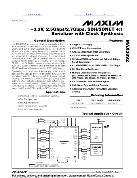
+3.3V, 2.5Gbps/2.7Gbps, SDH/SONET 4:1
Serializer with Clock Synthesis
MAX3892
AC ELECTRICAL CHARACTERISTICS (continued)
(V
CC
= +3.0V to +3.6V, T
A
= -40擄C to +85擄C. Typical values are at V
CC
= +3.3V, differential LVDS loads = 100鈩?鹵1%, CML loads =
50鈩?鹵1%, T
A
= +25擄C, unless otherwise noted.) (Note 3)
PARAMETER
Serial Clock Output Jitter
Generation
Serial Data Output Random Jitter
Serial Data Output Deterministic
Jitter
SYMBOL
JG
RJ
DJ
(Note 7)
(Note 6)
CONDITIONS
MIN
TYP
1.2
MAX
1.4
1.4
19
UNITS
ps
RMS
ps
RMS
ps
p-p
REFERENCE CLOCK INPUT SPECIFICATIONS
(RCLK)
Reference Clock Frequency
Tolerance
Reference Clock Input Duty Cycle
RESET INPUTS
(RESET)
Minimum Pulse Width of FIFO
Reset
Tolerated Drift Between PCLKI
and PCLKO After Reset
UI is PCLKO period
UI is PCLKO period
4
鹵1
UI
UI
鹵100
30
70
ppm
%
Note 1:
Note 2:
Note 3:
Note 4:
Specifications at -40擄C are guaranteed by design and characterization.
Measured with SLBO/CLK622 and SCLK outputs disabled and CML outputs open.
AC characteristics are guaranteed by design and characterization.
In 622MHz clock mode, the parallel data is clocked in by the rising edge of the 622MHz/666MHz parallel clock input. In the
311MHz clock mode, the parallel data is clocked in on both the rising and falling edges of the clock. The parallel input
setup and hold time increases by 60ps if the duty cycle is between 48% to 52% in 311MHz mode (Figure 1).
Note 5:
Relative to the falling edge of the SCLKO.
Note 6:
Measurement bandwidth is BW = 12kHz to 20MHz.
Note 7:
Deterministic jitter includes pattern-dependent jitter and pulse-width distortion. Measured using a 2
7
- 1 PRBS pattern with
96 consecutive identical digits.
4
_______________________________________________________________________________________


 1
1
 2
2
 3
3
 4
4
 5
5
 6
6
 7
7
 8
8
 9
9
 10
10
 11
11
 12
12
